AI's Insatiable Appetite: How the 2026 AI Chip Boom Is Reshaping Semiconductor Manufacturing
Table of Contents
⚡ Sourcing Summary
The generative AI boom is reorganizing the semiconductor industry in 2026. As TSMC CoWoS capacity remains constrained, secondary focus has moved to securing high-voltage power management ICs. Supply chain managers must secure mature and advanced logic allocations.
In February 2026, NVIDIA reported quarterly data center revenue of $38 billion—more than Intel and AMD’s combined total revenue for the same period. TSMC’s advanced packaging capacity is sold out through Q3 2027. OpenAI, Microsoft, Google, and Meta are designing their own AI accelerator ASICs, bypassing merchant silicon entirely for their highest-volume inference workloads. The AI chip revolution is no longer a forecast; it is the central organizing principle of the semiconductor industry.
The Numbers Behind the Boom
The scale of AI-driven semiconductor demand is difficult to overstate:
-
GPU and AI Accelerator Revenue: The merchant AI accelerator market (GPUs, FPGAs, and custom ASICs sold to third parties) reached $180 billion in 2025, according to Mercury Research and semiwiki estimates. NVIDIA commands approximately 80% of this market, with AMD’s Instinct MI400 series and Intel’s Gaudi 4 capturing most of the remainder.
-
HBM Memory: High-Bandwidth Memory has become a co-requisite for AI accelerators. SK Hynix, Samsung, and Micron collectively shipped over 800 million gigabytes of HBM3E memory in 2025. SK Hynix alone has committed $40 billion to HBM4 development and capacity expansion through 2030. HBM now accounts for approximately 25% of total DRAM industry revenue despite representing less than 5% of bit volume.
-
CoWoS and Advanced Packaging: TSMC’s Chip-on-Wafer-on-Substrate (CoWoS) capacity has more than tripled since 2023, reaching approximately 45,000 wafers per month by Q1 2026. Additional capacity from ASE/SPIL (FOCoS-B), Amkor (S-SWIFT), and Intel (EMIB) has not kept pace with demand. Advanced packaging remains the single most constrained node in the AI semiconductor supply chain.
-
Data Center Power: AI data center electricity consumption reached 65 terawatt-hours in 2025—roughly the annual electricity consumption of Switzerland. The International Energy Agency (IEA) projects this could reach 150 TWh by 2028, driven by the deployment of 100kW+ per-rack AI training clusters.
Advanced Packaging: The Real Bottleneck
While much of the public discourse focuses on leading-edge process nodes (3nm, 2nm), the binding constraint on AI chip production in 2026 is advanced packaging—specifically, the interposer-based integration technologies that marry compute chiplets with HBM stacks.
TSMC’s CoWoS-L (Chip-on-Wafer-on-Substrate with Local Silicon Interconnect) has become the de facto standard for AI accelerator packaging. A single NVIDIA B100 GPU module integrates:
- 2 compute chiplets (TSMC N3P, each ~400 mm²)
- 8 HBM3E stacks (each 12-Hi, 36 GB)
- 1 local silicon interconnect (LSI) bridge die
- 1 organic substrate (110mm × 110mm, 20+ layers)
The interposer alone requires 4-5 mask layers on a 65nm-class process, and each CoWoS-L wafer consumes roughly 1.5× the silicon area of the compute chiplets it integrates. This is manufacturing complexity of a different order than traditional monolithic packaging.
The capacity response has been dramatic but insufficient:
-
TSMC is building six dedicated advanced packaging facilities in Taiwan (AP6 through AP11), with AP6 and AP7 now in volume production. AP8, the first dedicated CoWoS-L-only fab, begins production in Q4 2026.
-
ASE Technology Holding (the world’s largest OSAT provider) has committed $6 billion to advanced packaging expansion, including its Fan-Out Chip-on-Substrate-Bridge (FOCoS-B) technology that offers CoWoS-like integration with different cost and capacity characteristics.
-
Samsung is pursuing a “unified packaging” strategy with its I-Cube and H-Cube platforms, integrating HBM with Exynos and third-party logic in a single package. Samsung’s ambition is to capture 15-20% of the non-TSMC AI accelerator packaging market by 2028.
-
Intel has opened its EMIB (Embedded Multi-die Interconnect Bridge) and Foveros Direct packaging technologies to foundry customers. Amazon’s AWS Inferentia 3 chip is the first significant external customer for Intel’s advanced packaging, manufactured on Intel 18A with EMIB integration of HBM.
The Rise of Custom AI ASICs
The hyperscalers are no longer content to buy NVIDIA’s products at NVIDIA’s prices. Every major cloud provider now has a custom silicon program:
-
Google’s TPU v6 (Trillium): Deployed at scale in 2025, fabricated on TSMC N3E with CoWoS-L packaging. Google uses TPUs for both internal workloads (search ranking, recommendation systems, Gemini model training) and external cloud customers via Google Cloud TPU instances. TPU v6 delivers approximately 2.3× the training throughput of TPU v5p for large language models.
-
Amazon’s Trainium 3 and Inferentia 3: Trainium 3, manufactured on Intel 18A (Amazon’s first non-TSMC AI chip), targets large-scale model training with 2 Tbps of aggregate memory bandwidth. AWS has committed to deploying over 500,000 Trainium 3 accelerators by late 2026.
-
Microsoft Azure Maia 3: Microsoft’s third-generation AI accelerator, fabricated on TSMC N3P, is optimized for GPT-class inference workloads. Microsoft has publicly stated that Maia 3 reduces the cost-per-token for GPT-5 inference by approximately 40% compared to equivalent NVIDIA H200 instances.
-
Meta’s MTIA v3: Meta’s in-house inference accelerator, used to power recommendation systems across Facebook, Instagram, and Threads. Unlike the training-focused designs from Google and Amazon, MTIA is optimized purely for inference at massive scale—Meta serves over 10 trillion inference queries per day.
-
OpenAI’s “Iris”: The most ambitious custom silicon program, OpenAI’s Iris chip (fabricated on TSMC N2 with custom HBM4 integration) began tape-out in late 2025 with first silicon expected in Q3 2026. Unlike the other hyperscaler ASICs, Iris may be offered to external customers, positioning OpenAI as a full-stack AI company from silicon to application layer.
The custom ASIC trend has profound implications for the semiconductor ecosystem. It concentrates leading-edge wafer and packaging demand among a handful of end-customers, crowds out smaller fabless companies from access to advanced nodes, and shifts value capture from merchant silicon vendors toward cloud providers and their internal design teams.
The Memory Wall and HBM4
The “memory wall”—the growing gap between compute throughput and memory bandwidth—is the central technical challenge for AI chip design in 2026. Large language models with trillions of parameters require memory bandwidth measured in terabytes per second, and traditional DDR5/LPDDR5 interfaces cannot approach these levels within reasonable power envelopes.
HBM4, standardized by JEDEC in early 2025, represents a step-change in memory interface technology:
- Bandwidth: 1.6 TB/s per stack (2048-bit interface at 6.4 Gbps per pin), double that of HBM3E
- Stack Height: Up to 16-Hi stacks with 48 GB per stack (up from 12-Hi/36 GB for HBM3E)
- Logic Base Die: HBM4 moves to a dedicated logic base die fabricated on a logic-compatible process, enabling on-die ECC, in-memory compute primitives, and adaptive training
- Power: Despite doubling bandwidth, HBM4 targets a 15% reduction in picojoules per bit through advanced signaling and 3D integration
The competitive dynamics in HBM have shifted. SK Hynix, historically the HBM market leader (supplying NVIDIA exclusively for H100/H200/B100 generations), now faces credible competition:
-
Samsung has qualified HBM3E for NVIDIA’s B100 and H200 platforms, and its HBM4 development is on an aggressive timeline targeting 2026 sampling. Samsung’s vertically integrated model (producing both logic and memory) gives it unique capability to co-optimize HBM logic base dies.
-
Micron has leapfrogged with HBM3E, shipping production volumes to NVIDIA for H200 GPUs. Micron’s decision to skip HBM3 entirely and go directly to HBM3E proved prescient, allowing it to capture approximately 15% of the HBM market by revenue in Q4 2025.
Power and Cooling: The Next Frontier
AI chip thermal design power (TDP) has crossed thresholds that require fundamental rethinking of data center power delivery and cooling:
-
A single NVIDIA B100 module draws approximately 1000W under full load. An 8-GPU HGX baseboard draws 8 kW. A fully populated rack with 8 HGX baseboards (64 GPUs) draws 72 kW—roughly the electrical load of 20 single-family homes.
-
This power density exceeds the limits of traditional air cooling. Direct-to-chip liquid cooling and immersion cooling have moved from niche to mainstream for AI deployments. Vertiv, a leading data center infrastructure supplier, reported in Q4 2025 that over 60% of new hyperscale data center capacity is being designed for liquid cooling from day one.
-
The concentration of AI workloads in specific geographies is straining electrical grids. Northern Virginia (the world’s largest data center market) has seen utility Dominion Energy impose moratoriums on new connections in certain substations. Ireland’s Commission for Regulation of Utilities has effectively capped new data center connections through 2028. AI chip energy efficiency—performance per watt—is now a purchasing criterion equal in importance to raw performance.
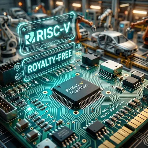
RISC-V and the Open Compute Ecosystem
The AI chip boom is driving adoption of RISC-V, not as a replacement for x86 or Arm in the application processor, but as the control-plane and management-plane architecture within AI accelerators:
-
NVIDIA’s B100 and H200 GPUs each contain over 40 RISC-V cores handling power management, thermal monitoring, fault detection, and security functions. This is invisible to the programmer but essential to the silicon architecture.
-
RISC-V-based AI accelerators are emerging from startups (Tenstorrent, Esperanto, Ventana) and established players (Samsung, Alibaba/T-Head). These are not yet competitive with NVIDIA GPUs or hyperscaler ASICs for training workloads, but they are gaining traction in inference at the edge and in cost-sensitive data center deployments.
-
The U.S. Department of Defense has mandated RISC-V for all new secure processing programs under the Trusted and Assured Microelectronics (T&AM) program, citing the architecture’s openness and the ability to perform comprehensive formal verification.
Implications for the Electronics Supply Chain
The AI chip boom has spillover effects throughout the electronics supply chain:
-
Leading-Edge Wafer Allocation: TSMC’s N3 and N2 nodes are effectively sold out through 2027. Smaller fabless companies without the purchasing power of NVIDIA, Apple, or the hyperscalers face extended lead times and unfavorable wafer pricing. Some are migrating designs to Samsung or Intel Foundry Services, accelerating the multi-foundry trend.
-
Advanced Substrate Shortages: The organic substrates used in AI accelerator packages (110mm × 110mm and larger, 20+ layers, ultra-low CTE) are produced by a limited number of suppliers (Unimicron, Ibiden, Shinko, AT&S). Capacity expansion is capital-intensive and slow. Substrate availability will constrain AI chip production through at least 2027.
-
Passive Component Demand: Each AI accelerator module requires hundreds of MLCCs (Multi-Layer Ceramic Capacitors), inductors, and precision resistors for power delivery and signal integrity. The sheer volume of AI chip production has tightened supply for high-frequency, high-temperature MLCCs (C0G/NP0 dielectrics, 0402 and smaller), with lead times extending from 8 weeks to 26+ weeks for certain values.
-
Test and Inspection: AI chips with 100+ billion transistors require exhaustive test coverage. Advantest and Teradyne have reported record backlogs for high-end SoC testers, with lead times exceeding 12 months. The test cost for a single B100 GPU module is estimated at $80-120, and test time (including burn-in) can exceed 4 hours per module.
Looking Ahead
The AI chip boom is not a bubble—it is a structural transformation of the semiconductor industry driven by the most significant new workload since the smartphone. Every leading-edge wafer, every square millimeter of advanced packaging capacity, and every gigabyte of HBM will be consumed by AI demand for the foreseeable future.
The implications are far-reaching:
-
Concentration Risk: The AI chip supply chain is dangerously concentrated—TSMC for wafers, TSMC for packaging, and SK Hynix for HBM. Any disruption at any of these nodes has global consequences. Diversification is essential but will take years.
-
Legacy Node Neglect: As capital flows overwhelmingly toward leading-edge AI infrastructure, legacy nodes (28nm and above) that serve automotive, industrial, and defense applications face underinvestment. This will create shortages in “boring” but essential chips.
-
Geopolitical Dimension: The concentration of AI chip manufacturing in Taiwan, combined with China’s exclusion from advanced node access through export controls, has made semiconductor manufacturing the most geopolitically consequential industry on Earth.
For procurement professionals, the message is clear: the AI chip boom affects your supply chain, even if you’re not buying GPUs. Advanced packaging capacity consumed by AI is capacity not available for other advanced ICs. Wafer starts allocated to hyperscaler ASICs are starts not available for your networking processor or FPGA. The second-order effects of AI demand on the broader semiconductor supply chain will be felt for the rest of this decade.
SupplyICs tracks AI semiconductor supply chain developments through dedicated industry monitoring. Our procurement specialists can assist with sourcing AI-adjacent components, assessing lead time impacts, and developing alternative sourcing strategies for components affected by AI-driven capacity constraints.
SupplyICs Sourcing Team
Contact Our TeamIndependent Component Specialists
A team of veteran buyers navigating the global spot market. We specialize in locating hard-to-find, shortage, and EOL components. From strict anti-counterfeit verification to cross-reference matching, we provide frontline data to help you secure authentic stock safely.