Table of Contents
- CoWoS Capacity: By the Numbers (June 2026 Update)
- Where Is the New Capacity Coming From?
- Introducing CoPoS: What Changes and What Doesn’t
- The CoWoS Silicon Interposer Problem
- The CoPoS Solution: Panel-Based Organic Substrates
- CoPoS Timeline
- What Does the CoWoS-to-CoPoS Transition Mean for Procurement?
- For AI Accelerator Buyers (OEMs, Cloud Providers)
- For Component Buyers (Passives, Connectors, Thermal Solutions)
- The Bottom Line
In the first half of 2024, the CoWoS shortage was the single biggest constraint on AI chip supply. NVIDIA could sell every H100 it could package, and packaging capacity—not logic wafer capacity—was the limiting factor.
Two years later, the narrative has shifted. The question is no longer “Can the industry produce enough advanced packaging capacity?” It is “When does the capacity expansion overtake demand growth—and what does the next-generation technology platform mean for packaging allocation?”
📌 Direct Answer: CoWoS supply-demand balance is improving along two vectors: TSMC's aggressive capacity expansion (140K wpm targeted, 3x from 2023) and OSAT partner capacity coming online (ASE, SPIL, and Powertech collectively adding 50K-60K wpm of CoWoS-compatible advanced packaging capacity). TrendForce's June 2026 data shows the gap narrowed from 20% to 10%—meaning roughly 90% of CoWoS demand can be met, up from 80% a year ago. The next-generation platform, CoPoS, shifts from silicon interposer to panel-based organic substrate technology, enabling 5x larger package areas at 40% lower cost per unit area—but requires an entirely new manufacturing line. CoPoS will not relieve CoWoS pressure in 2026-2027; it is a 2028+ technology. Procurement teams should plan for constrained but incrementally improving CoWoS access through 2027, with the CoPoS transition creating new options from 2028.
Related Reading: For the foundational CoWoS bottleneck analysis from earlier in 2026, see CoWoS Is the New Silicon Shortage: What Procurement Teams Must Know About the 2026 Packaging Crisis. This article provides the June 2026 capacity update and introduces the CoPoS transition. For the AI chip market context, see AI Chip Boom: Semiconductor Industry Transformation 2026.
CoWoS Capacity: By the Numbers (June 2026 Update)
TrendForce’s June 15, 2026 advanced packaging monitor provides the most detailed public data on CoWoS capacity and utilization:
| Parameter | End of 2024 | Mid-2025 | End of 2025 | Mid-2026 | End of 2026 (Projected) |
|---|---|---|---|---|---|
| TSMC CoWoS (wpm) | ~50,000 | ~80,000 | ~100,000 | ~120,000-140,000 | ~150,000-160,000 |
| OSAT Partners (wpm) | ~5,000 | ~15,000 | ~25,000 | ~50,000-60,000 | ~60,000-70,000 |
| Total CoWoS Capacity (wpm) | ~55,000 | ~95,000 | ~125,000 | ~170,000-200,000 | ~210,000-230,000 |
| Demand (wpm equivalent) | ~70,000 | ~110,000 | ~150,000 | ~190,000-220,000 | ~220,000-260,000 |
| Supply-Demand Gap | ~20% shortfall | ~15% shortfall | ~18% shortfall | ~10% shortfall | ~10% shortfall (est.) |
| CoWoS Lead Time (new customers) | 52+ wks, allocation closed | 40-52 wks | 30-40 wks | 26-36 wks | 20-30 wks (est.) |
Sources: TrendForce (June 15, 2026), CNBC (April 8, 2026), Digitimes, TSMC earnings calls, SupplyICs analysis.
The key takeaways:
-
Capacity roughly tripled from end-2023 to mid-2026. TSMC converted significant portions of its Fab 12, Fab 14, Fab 15, and Fab 18 cleanroom space to CoWoS lines, and built dedicated CoWoS capacity at its new Tongluo (Miaoli) and Chiayi (planned) advanced packaging campuses.
-
OSAT partners are no longer a rounding error. ASE and SPIL together now represent approximately 30% of total CoWoS-compatible capacity. This is transformative for procurement: a year ago, CoWoS was effectively a TSMC monopoly. Today, there are multiple packaging suppliers capable of certain CoWoS process steps, which improves both allocation availability and pricing leverage.
-
Demand grew faster than capacity throughout 2024-2025, but the gap is finally narrowing. The 10% gap in mid-2026—down from 20% at start-of-year—suggests capacity expansion is about to overtake demand growth for the first time since the AI boom began.
Where Is the New Capacity Coming From?
TSMC has built or converted CoWoS capacity at four sites:
- AP6 (Tongluo Science Park, Miaoli, Taiwan): The first dedicated CoWoS-only facility. Phase 1 reached 30,000 wpm in Q1 2026; Phase 2 is under construction targeting 30,000 additional wpm by end-2027.
- Fab 12 (Hsinchu, Taiwan): TSMC’s original advanced packaging site. CoWoS lines have been expanded into former 300mm logic cleanroom space, adding approximately 20,000 wpm.
- Fab 14 (Tainan, Taiwan): CoWoS lines added alongside the 3nm/5nm logic fab, primarily supporting NVIDIA and AMD packaging demand.
- Fab 18 (Tainan, Taiwan): Newest CoWoS expansion, primarily serving Apple and hyperscaler custom silicon (Amazon Trainium, Google TPU).
In addition, ASE (Kaohsiung, Taiwan), SPIL (Taichung, Taiwan), and Powertech (Hsinchu, Taiwan) have all qualified CoWoS-compatible processes, primarily handling the “oS” (on-substrate) portion of the CoWoS flow: silicon interposer attachment to organic BGA substrate, underfill, and lid attach. The CoW (chip-on-wafer) portion—the microbump bonding and chip-on-interposer assembly—remains primarily TSMC in-house, though ASE has announced qualification of CoW processes for non-NVIDIA customers.
Introducing CoPoS: What Changes and What Doesn’t
CoPoS (Chip-on-Panel-on-Substrate) is TSMC’s designated successor to CoWoS for the largest, most complex AI accelerator packages. The name change from “Wafer” to “Panel” signals the fundamental architectural shift.
The CoWoS Silicon Interposer Problem
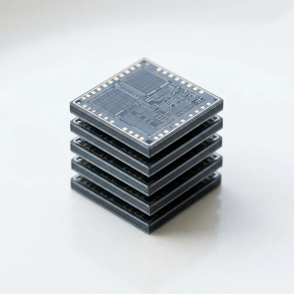
CoWoS uses a silicon interposer—a large passive silicon chip fabricated on a logic process—as the interconnection layer between logic chiplets and HBM stacks. Silicon interposers are electrically ideal (fine pitch microbumps, low-loss through-silicon vias) but have a fundamental economic problem: they consume silicon wafer area.
The largest CoWoS interposer currently in production—the 3.3x reticle size interposer used for NVIDIA B200 (approximately 2,800mm²)—requires almost an entire 300mm wafer to produce just 25-30 interposers (accounting for the rectangular interposer shape vs. round wafer). The interposer alone accounts for roughly 25-30% of the total CoWoS packaging cost.
The CoPoS Solution: Panel-Based Organic Substrates
CoPoS replaces the silicon interposer with a large-format organic substrate fabricated using panel-level processes (510mm × 515mm panels, similar to flat-panel display manufacturing). The panel format provides approximately 5x the usable area of a 300mm silicon wafer, and the organic substrate manufacturing process (build-up layers of Ajinomoto Build-up Film or equivalent dielectric with semi-additive copper plating) is inherently lower cost than silicon wafer processing.
The trade-off is line/space capability: CoPoS organic substrates achieve approximately 1.5µm line/space (vs. 0.4µm for CoWoS silicon interposers), which limits die-to-die interconnect density. For AI accelerator applications where the logic-to-HBM interface is the bandwidth-critical path, the 1.5µm line/space is sufficient because HBM interface bumps are typically 25-35µm pitch, which is compatible with organic substrate routing.
The cost advantage is compelling: TrendForce estimates CoPoS packaging cost for a 10,000mm² multi-chip module at approximately 40% below equivalent CoWoS cost, driven primarily by eliminating the expensive silicon interposer.
CoPoS Timeline
| Milestone | Timeline | Status |
|---|---|---|
| R&D feasibility demonstration | 2024-2025 | ✅ Completed |
| Process qualification at VisEra | Q2 2026 | ✅ Completed (Commercial Times, June 15, 2026) |
| Pilot production line installation | H2 2026 | In progress |
| First customer tape-out (NVIDIA Feynman test vehicle) | H1 2027 | Planned |
| Pilot production | Mid-2027 | Planned |
| Mass production (NVIDIA Feynman) | 2028-2029 | Target |
CoPoS is not a 2026 procurement reality—it is a 2028+ technology. But it matters for procurement planning now because it will eventually bifurcate the advanced packaging market: cutting-edge AI accelerators moving to CoPoS (freeing up CoWoS capacity for the broader market), while existing-design AI chips remain on CoWoS. The procurement teams that understand this transition pathway will be better positioned to negotiate CoWoS allocation as the capacity mix shifts.
What Does the CoWoS-to-CoPoS Transition Mean for Procurement?
For AI Accelerator Buyers (OEMs, Cloud Providers)
If you are buying NVIDIA H200/B200/GB200 systems, or AMD MI300X/MI400 systems, or custom ASICs (AWS Trainium, Google TPU) that use CoWoS packaging, the capacity outlook depends on your volume tier:
- Hyperscalers (50,000+ units/year): You already have CoWoS allocation. Your near-term concern is transition planning—when does your silicon roadmap migrate from CoWoS to CoPoS, and how do you manage the packaging qualification and yield ramp of the new platform?
- Tier-2 cloud/enterprise (5,000-50,000 units/year): CoWoS access is improving. OSAT partners are your unlocking path—ask your silicon supplier whether ASE/SPIL CoWoS-compatible capacity is qualified for your product. If not, push for qualification. The OSAT option is the fastest path to incremental capacity.
- Startups/small volume (<5,000 units/year): CoWoS access remains challenging. Consider whether your AI accelerator product can be architected to use standard flip-chip packaging (no silicon interposer, direct die-to-substrate attach) for initial production while waiting for CoWoS/CoPoS allocation to broaden. Several AI chip startups have successfully shipped initial silicon on standard flip-chip before transitioning to advanced packaging for production scaling.
For Component Buyers (Passives, Connectors, Thermal Solutions)
CoPoS packages will be larger and dissipate more power than CoWoS packages. The NVIDIA Feynman platform is expected to integrate 8-12 chiplets in a package exceeding 10,000mm², with total package power of 2-3kW. This creates demand for new categories of components:
- High-current power delivery: More package pins dedicated to power delivery, driving demand for finer-pitch socket connectors and higher phase-count voltage regulators.
- Advanced thermal solutions: 2-3kW per package pushes air cooling past its practical limit, accelerating direct-to-chip liquid cooling and immersion cooling adoption.
- High-density passives: More chiplets means more decoupling capacitance per package, driving demand for silicon capacitors and low-ESL MLCCs with tighter placement.
These are secondary procurement effects, but they will materialize alongside the CoPoS transition in the 2028-2030 timeframe.
The Bottom Line
The CoWoS crisis—the period when advanced packaging was the dominant constraint on AI chip supply—is transitioning into a managed-shortage phase. Capacity has roughly tripled since 2023; OSAT partners have emerged as credible alternative suppliers; and the CoPoS R&D pipeline provides a path to fundamentally lower packaging costs for next-generation designs.
For procurement, the message is cautiously optimistic: CoWoS access will continue improving incrementally through 2027, and the CoPoS transition will accelerate the improvement from 2028 onward. The days of “CoWoS allocation closed” are ending. The era of “CoWoS allocation available at a price” is beginning.
SupplyICs tracks advanced packaging capacity, lead times, and allocation across TSMC CoWoS/CoPoS, ASE/SPIL, Samsung I-Cube, and Intel EMIB platforms. Contact our market intelligence team for analysis of how advanced packaging allocation affects your specific AI hardware procurement requirements.
Frequently Asked Questions (FAQ)
What is the current CoWoS capacity and supply-demand gap in mid-2026?
TSMC's CoWoS (Chip-on-Wafer-on-Substrate) advanced packaging capacity reached approximately 120,000-140,000 wpm (wafer starts per month) in mid-2026, plus 50,000-60,000 wpm from OSAT partners (ASE, SPIL, Powertech). The supply-demand gap has narrowed from approximately 20% in late 2025 to roughly 10%, according to TrendForce's June 15, 2026 analysis—meaning demand still exceeds supply by about 10%, down from 20%, but no longer at crisis levels. The improvement is driven by TSMC's aggressive capacity expansion (CoWoS capacity has roughly tripled since 2023) and some demand diversification as Intel's EMIB and Samsung's I-Cube gain share for non-NVIDIA AI accelerator packaging.
What is CoPoS and how does it differ from CoWoS?
CoPoS (Chip-on-Panel-on-Substrate) is TSMC's next-generation advanced packaging platform that replaces the silicon interposer used in CoWoS with a larger, lower-cost panel-based substrate—similar to the organic substrates used in standard flip-chip packaging but with significantly finer line/space capability (1.5µm vs 8-10µm for standard organic substrates). The panel format (510mm × 515mm) enables roughly 5x the interposer area of the largest CoWoS silicon interposer (3.3x reticle, approximately 2,800mm²) at approximately 40% lower cost per unit area. CoPoS targets the next generation of AI accelerators—NVIDIA's Feynman platform (2028-2029), which is expected to integrate 8-12 chiplets with HBM4 memory stacks on a single package exceeding 10,000mm² in total area. CoPoS completed R&D qualification in June 2026, with pilot production planned for mid-2027.
When will CoWoS allocation ease enough for non-hyperscaler AI chip companies to access capacity?
Non-hyperscaler access to CoWoS capacity is improving but remains constrained through at least Q2 2027. The capacity pipeline is encouraging: TSMC's CoWoS capacity will grow from 120K-140K wpm (mid-2026) to an estimated 180K-200K wpm by end of 2027 as new CoWoS lines at TSMC's Tongluo and Chiayi sites ramp. However, NVIDIA alone is estimated to consume 45-55% of total CoWoS capacity in 2026, and orders from AMD, Intel, Broadcom, Amazon (Trainium), Google (TPU), and Microsoft (Maia) account for most of the remainder. For fabless AI chip startups and mid-size companies, meaningful CoWoS allocation availability is realistically a 2028 story—when the combination of continued TSMC expansion, increased OSAT partner capacity, and the initial migration of highest-end designs to CoPoS opens up capacity in the CoWoS segment.