Table of Contents
- Why Is AI GPU Burn-In Testing the Defining Demand Driver for the IC Socket Market in 2026?
- How Are Technology Transitions Reshaping the Test and Burn-In Socket Landscape?
- What Is Driving the Shift from Spring-Loaded Pogo-Pin Sockets to Elastomer Contact Technology?
- How Are LGA Sockets Displacing Traditional BGA Sockets in AI Test Applications?
- What Is the Real State of Burn-In Socket Lead Times and Pricing in Q3 2026?
- Socket Type Comparison: Lead Times, Costs, and Lifespans
- Why Are Japanese Suppliers Dominating the Premium Burn-In Socket Segment?
- How Does the Burn-In Socket Shortage Connect to the Broader Advanced Packaging Crisis?
- What Are the Thermal and Mechanical Requirements Driving Burn-In Socket Complexity?
- Why Does High-Temperature Burn-In Demand Such Specialized Socket Materials?
- How Are Test Socket Thermal Solutions Evolving to Meet AI Chip Requirements?
- What Should Procurement Teams Do Now to Secure Burn-In Socket Supply?
- How Should You Build a Multi-Supplier Burn-In Socket Qualification Strategy?
- How Should You Manage Burn-In Socket Inventory as a Consumable, Not a Capital Item?
A semiconductor test house in Malaysia recently approached us when their burn-in socket order from a major Japanese supplier was pushed from 12 weeks to 34 weeks. They had 14 burn-in boards for a next-generation AI accelerator — each board carrying 12 custom BGA sockets — and three sockets had already failed beyond repair. Without replacements, they were looking at 21% capacity loss on a $4 million quarterly test contract. Through our network of secondary suppliers in South Korea and Taiwan, we sourced 40 functional equivalents with identical spring-probe geometry and PEEK insulator ratings within 18 days, including the necessary 3D metrology validation. This is not an outlier. It is the new normal in the IC socket market, and it demands a fundamentally different procurement playbook.
Why Is AI GPU Burn-In Testing the Defining Demand Driver for the IC Socket Market in 2026?

The IC socket market has historically been a steady, predictable segment of the semiconductor supply chain — growing roughly in line with overall chip unit volumes. That predictability vanished in 2025. The single largest disruptor is the explosive growth in AI GPU burn-in testing, which has fundamentally reshaped how socket manufacturing capacity is allocated, priced, and prioritized across the entire industry.
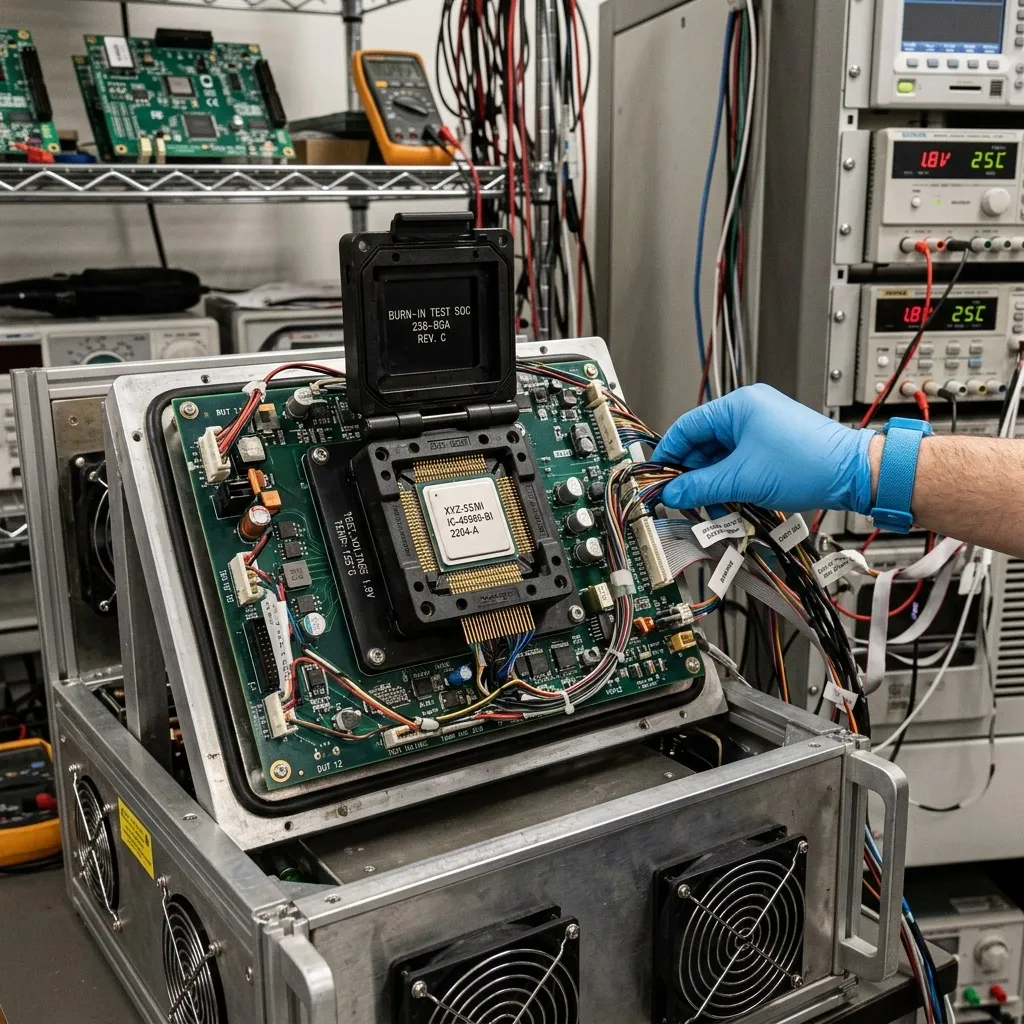
Every high-performance AI accelerator — whether an NVIDIA H200, an AMD MI300X, or a custom cloud ASIC — must undergo burn-in testing before deployment. Burn-in is not optional. It is a reliability gate that exposes early-life failures by operating chips at elevated temperatures (typically 125C to 175C) and voltages for 24 to 72 continuous hours. For AI GPUs with retail prices exceeding $30,000 per unit and deployed in clusters of 10,000 or more, the cost of a field failure is catastrophic. Hyperscalers demand zero-defect screening, and that screening runs through burn-in sockets.
What changed in 2025-2026 is volume. According to SEMI’s Q2 2026 packaging materials outlook, AI GPU burn-in testing demand surged 45% year-over-year. NVIDIA alone shipped an estimated 2.5-3 million datacenter GPUs in 2025, each requiring 48+ hours of burn-in. At any given moment, tens of thousands of burn-in sockets are actively cycling AI chips through thermal stress testing. This sustained, high-utilization consumption of precision sockets — combined with the fact that burn-in sockets are consumable items with finite lifespans — has created demand that the socket supply base was not dimensioned to serve.
How Are Technology Transitions Reshaping the Test and Burn-In Socket Landscape?
The technology evolution in IC sockets is accelerating under the pressure of AI chip requirements. The industry is undergoing a multi-dimensional transition — from DIP to BGA to LGA to elastomer sockets — and each transition has implications for availability, cost, and supplier qualification timelines.
What Is Driving the Shift from Spring-Loaded Pogo-Pin Sockets to Elastomer Contact Technology?
Traditional burn-in and test sockets rely on spring-loaded pogo-pin contacts: gold-plated beryllium-copper probes with internal springs that compress to make electrical contact with each device pad. This technology has been the workhorse of semiconductor testing for three decades. It works. It is well-understood. It is also, for the newest generation of AI GPUs, reaching its physical limits.
The problem is pitch. As AI GPU packages grow larger — 60mm x 60mm body sizes are now common, with 70mm+ on the horizon — and pin counts climb past 5,000-7,000 contacts, the mechanical tolerances required for pogo-pin alignment become punishingly expensive to machine. At 0.35mm pitch and below, spring probes must be fabricated with single-micron precision, and the cumulative thermal expansion mismatch between the socket body, the contacts, and the device PCB at 150C+ creates reliability challenges that pogo-pin designs struggle to solve.
Elastomer contact technology offers an alternative. Instead of individual spring probes, elastomer sockets use a conductive silicone or metal-particle-impregnated polymer sheet that compresses between the device and the test board. The elastomer deforms to make contact with every pad simultaneously, distributing contact force evenly across the entire device footprint. Key advantages include: zero insertion force (ZIF) compatibility, higher contact density at fine pitches, better thermal conductivity through the elastomer matrix, and simpler mechanical construction that reduces CNC machining requirements by 40-60% compared to equivalent pogo-pin designs.
The trade-off is lifespan. Elastomer contacts typically deliver 50,000-200,000 insertions before replacement, compared to 500,000-1,000,000 for high-quality spring probes. For development and low-volume production testing, this is acceptable. For high-volume manufacturing burn-in running 24/7, the shorter replacement interval can translate to higher total cost of ownership despite lower upfront socket cost.
How Are LGA Sockets Displacing Traditional BGA Sockets in AI Test Applications?
The transition from BGA (Ball Grid Array) to LGA (Land Grid Array) packaging for AI processors is directly reshaping socket technology requirements. BGA packages have solder balls on the underside that make permanent connections to the PCB; BGA test sockets must accommodate these balls without damaging them, which demands precision-machined spring-probe nests or clamshell designs that add cost and complexity.
LGA packages, by contrast, present flat contact pads rather than solder balls. This simpler interface geometry enables lower-profile socket designs, better signal integrity at high frequencies (reduced parasitic inductance from shorter contact paths), and — critically — compatibility with elastomer contact sheets that are inherently better suited to flat-pad interfaces than to spherical solder ball interfaces.
NVIDIA’s Grace Hopper superchip module, Intel’s Gaudi 3 accelerator, and AMD’s MI300-series all use LGA or LGA-hybrid interfaces. As LGA adoption grows across the AI accelerator landscape, socket suppliers who have invested in elastomer and hybrid LGA socket platforms — notably Enplas and ISC Technology — are gaining share, while traditional pogo-pin specialists face pressure to adapt their product lines. For procurement teams, this means that the socket your engineering team qualified 18 months ago may no longer be the optimal choice, and the supplier landscape for LGA-compatible burn-in sockets is materially different from the BGA socket supplier base.
What Is the Real State of Burn-In Socket Lead Times and Pricing in Q3 2026?
The question every procurement manager is asking right now: how long will I actually wait, and how much will I actually pay? The answer depends heavily on socket type, supplier tier, and your organization’s relationship depth with the manufacturer.
Socket Type Comparison: Lead Times, Costs, and Lifespans
| Socket Type | Typical Lead Time (Q3 2026) | Unit Cost Range | Insertion Lifespan | Key Suppliers | Primary Application |
|---|---|---|---|---|---|
| BGA Burn-In Socket (Custom) | 28-34 weeks | $800-$1,500 | 500K-1M cycles | Yamaichi, Enplas, Smiths Connectors | AI GPU/ASIC high-volume production burn-in |
| BGA Test Socket (Standard) | 18-24 weeks | $300-$700 | 100K-300K cycles | Cohu, Johnstech, Ironwood | Device characterization, qualification testing |
| Elastomer Burn-In Socket | 16-22 weeks | $400-$900 | 50K-200K cycles | ISC Technology, Leeno, Enplas | LGA-package burn-in, fine-pitch applications |
| Production Socket (BGA/LGA) | 8-14 weeks | $20-$150 | 50-500 cycles | TE Connectivity, Molex, Aries, Mill-Max | Permanent or semi-permanent device mounting |
| Development/Debug Socket | 4-8 weeks | $150-$500 | 10K-50K cycles | Ironwood, Aries, 3M Textool, Enplas | Lab characterization, firmware development |
| DIP Microcontroller Socket | 18-24 weeks | $0.30-$3.00 | 50-200 cycles | TE Connectivity, 3M, Mill-Max, Winslow | Legacy industrial, through-hole applications |
The cost escalation is concentrated in the custom burn-in socket segment, where AI demand is most acute. A custom BGA burn-in socket for a 55mm+ AI GPU package with 4,000+ pins and 0.4mm pitch now commands $1,200-$1,500 from a Tier-1 Japanese supplier — roughly 2x the 2023 price for equivalent complexity. Even standard catalog burn-in sockets that were $200-400 in 2023 are now routinely quoted at $350-600, reflecting both raw material inflation (high-temperature polymers, gold plating) and the simple reality that every CNC spindle hour that could be spent on a $1,200 custom socket will not be spent on a $350 standard socket.
Why Are Japanese Suppliers Dominating the Premium Burn-In Socket Segment?
Yamaichi Electronics and Enplas Corporation have built multi-decade franchises in high-reliability test sockets through a combination of in-house precision machining, proprietary contact metallurgy, and deep co-engineering relationships with the world’s largest semiconductor manufacturers. Yamaichi’s spring-probe fabrication capability — producing contacts with sub-micron dimensional tolerances, precisely controlled spring forces, and proprietary gold-alloy plating formulas — is not easily replicated. Enplas’ elastomer and LGA socket platforms benefit from the company’s parallel expertise in precision injection molding of engineering polymers, a competency that most pure-play socket manufacturers lack.
The result is a market structure where the top two Japanese suppliers command an estimated 45-50% share of AI-grade burn-in socket revenue, with lead times that set the ceiling for the entire industry. When Yamaichi quotes 34 weeks, competing suppliers raise their own lead times to 22-26 weeks because they know demand will flood toward them. This is not collusion; it is a capacity-constrained market responding rationally to overwhelming demand.
Smiths Connectors (UK/US) and Cohu (US) serve as the primary Western alternatives, with strong positions in specific test platform ecosystems. Smiths’ IDI brand spring probes are widely specified in Teradyne and Advantest test handlers, creating an installed-base moat that makes it difficult for procurement teams to switch suppliers without requalifying the entire test cell. Cohu’s acquisition of Rasco in 2023 integrated socket design with test handler engineering, offering an integrated solution that appeals to large OSATs but creates vendor lock-in risk.
How Does the Burn-In Socket Shortage Connect to the Broader Advanced Packaging Crisis?
The burn-in socket shortage does not exist in isolation. It is a downstream consequence of the same forces creating the CoWoS advanced packaging bottleneck that we analyzed in our detailed CoWoS supply chain report. Understanding this connection is essential for procurement teams who need to forecast their total test infrastructure requirements accurately.
The causal chain works as follows: TSMC, Amkor, and Intel Foundry Services are racing to expand CoWoS and equivalent 2.5D/3D packaging capacity. Every new CoWoS production line that comes online — and TSMC is targeting 120,000-140,000 wafers per month by late 2026 — generates a proportional requirement for burn-in test capacity downstream. Each wafer produces dozens of individual AI GPU packages, each of which must be burned in. The socket demand generated by new packaging capacity is therefore multiplicative: one new CoWoS line drives demand for thousands of additional burn-in sockets across the test supply chain.
At the same time, the advanced packaging substrates used in CoWoS and competing platforms share raw material supply chains with high-performance IC sockets. The ultra-flat, high-thermal-stability organic substrates and silicon interposers that make CoWoS possible require the same engineering-grade polymers (LCP, BT resin, polyimide) that go into burn-in socket insulators. When TSMC places a blanket order for substrate materials that consumes 60% of global high-grade LCP supply, socket manufacturers find themselves competing for the remainder — and losing.
This is why the conventional wisdom that “socket shortages are temporary” may be wrong this cycle. The capacity expansion in advanced packaging is structural and multi-year, and the socket demand it generates is proportional to that expansion. Until the socket manufacturing base expands its own precision machining and elastomer molding capacity — a process that takes 18-24 months for new CNC equipment installation and operator training — the imbalance between burn-in socket supply and AI-driven demand will persist.
Our earlier coverage of the general IC socket market lead time situation provides additional context on how the broader socket supply chain is responding, including cross-reference strategies and multi-source qualification approaches that apply across socket categories. This article focuses specifically on the AI burn-in testing segment, which is the acute pressure point within the broader socket market.
What Are the Thermal and Mechanical Requirements Driving Burn-In Socket Complexity?
Burn-in testing is fundamentally a thermal stress exercise. The socket is not merely an electrical interconnect — it is a thermal interface, a mechanical fixture, and a signal integrity element, all operating simultaneously at 150C to 175C for tens of thousands of cumulative hours over its service life. Understanding the specific requirements helps explain why lead times are long and why not every socket manufacturer can serve this market.
Why Does High-Temperature Burn-In Demand Such Specialized Socket Materials?
At 150C, standard FR4 PCB material begins to degrade. At 175C, even high-Tg FR4 is operating near its glass transition temperature, where mechanical stability cannot be guaranteed. Burn-in sockets must maintain dimensional stability, contact force consistency, and electrical insulation resistance at temperatures that would destroy commodity materials — and they must do so for hundreds of thousands of thermal cycles from ambient to 150C+ and back.
This demands engineering polymers that occupy a specific intersection of properties: high continuous-use temperature (above 200C), low coefficient of thermal expansion (CTE) matched to silicon and ceramic substrates, high dielectric strength, low moisture absorption, and machinability to micron-level tolerances. The shortlist of viable materials is dominated by:
- Torlon (PAI): Continuous-use temperature of 260C, excellent machinability, but expensive ($80-120/kg) and requires post-machining curing to achieve full mechanical properties
- PEEK: Continuous-use temperature of 250C, excellent chemical resistance, lower moisture absorption than Torlon, but harder to machine to sub-micron tolerances
- Vespel (PI): Continuous-use temperature of 300C, the gold standard for extreme thermal applications, but costs $200-400/kg and is available from a single primary supplier (DuPont)
- LCP (Liquid Crystal Polymer): Good balance of properties for applications below 200C, lower cost than PEEK/PI, but anisotropic CTE requires careful mold flow design
The supply of these materials is itself constrained. Global PEEK production is dominated by Victrex (UK) and Solvay (Belgium), with combined annual capacity of approximately 15,000 metric tons. Aerospace, medical implant, and oil-and-gas applications consume roughly 70% of this output. Socket manufacturers are competing for the remaining 30% against semiconductor capital equipment, automotive sensor, and specialty connector applications — and losing ground as AI-driven demand accelerates.
How Are Test Socket Thermal Solutions Evolving to Meet AI Chip Requirements?
The thermal management challenge goes beyond material selection. AI GPUs dissipate 700-1,000W during normal operation. During burn-in — with elevated voltages and ambient temperatures already at 125-150C — the junction temperature can approach 175-185C, right at the edge of silicon reliability limits. The burn-in socket must not only survive these temperatures but actively contribute to thermal management by providing a low-resistance thermal path from the device to the burn-in board’s cooling infrastructure.
This is driving the emergence of “active thermal socket” designs that integrate heat spreaders, vapor chambers, or even microfluidic cooling channels directly into the socket body. Persistence Market Research projects the test socket thermal solutions market growing from $1.8 billion in 2026 to $3.0 billion by 2033 at 7.6% CAGR — a growth rate that significantly outpaces the broader socket market, confirming that thermal capability is becoming the primary differentiator in burn-in socket procurement.
For procurement teams, the practical implication is that burn-in socket specifications are becoming more complex and more application-specific. A socket qualified for NVIDIA H100 burn-in at 125C ambient may not be suitable for H200 burn-in at 150C ambient, even if the package dimensions are identical. Thermal derating curves, contact resistance stability across temperature, and insulator material certifications must be reviewed with engineering before any cross-reference or second-source qualification is attempted.
What Should Procurement Teams Do Now to Secure Burn-In Socket Supply?
The IC socket market is not going to normalize in 2026. With AI GPU production volumes still scaling, CoWoS capacity still expanding, and socket manufacturing capacity constrained by both precision machining equipment lead times and skilled operator availability, the supply-demand imbalance will persist through at least Q2 2027. Here is what procurement teams should do immediately.
How Should You Build a Multi-Supplier Burn-In Socket Qualification Strategy?
Single-sourcing burn-in sockets from a Tier-1 Japanese supplier was viable when lead times were 8-12 weeks and demand was predictable. It is not viable when lead times are 28-34 weeks and your supplier’s largest customer (NVIDIA or an NVIDIA contract manufacturer) can preempt your allocation at any time.
The minimum viable approach in 2026 is dual-source qualification. Identify a primary supplier (likely Yamaichi or Enplas if your test infrastructure is already built around their socket footprints) and a secondary supplier (ISC Technology, Leeno, or Johnstech) that can produce mechanically and electrically equivalent sockets. The qualification process should include:
- 3D Metrology Validation: Confirm that the secondary socket’s contact positions, planarity, and insertion depth match the primary socket within the tolerances specified by your device datasheet. Budget 2-3 weeks.
- Electrical Characterization: Measure contact resistance, inductance, and capacitance across the full pin count at both ambient and 150C+. Budget 3-4 weeks including thermal chamber time.
- Insertion Lifecycle Testing: Run 50,000-100,000 insertion cycles (or your expected quarterly consumption, whichever is higher) and monitor contact resistance drift. Budget 4-6 weeks depending on available test automation.
- Device Yield Correlation: Run a statistically significant sample of devices through burn-in using both primary and secondary sockets, and compare yield and fallout patterns. Budget 2-3 weeks plus device availability.
Total qualification timeline: 11-16 weeks. If you start today, you have a qualified second source by late October 2026. If you wait until your primary supplier issues a force majeure or decommit notice, you will be 11-16 weeks from having an alternative — and during those weeks, your test capacity will be degraded by however many sockets have failed.
How Should You Manage Burn-In Socket Inventory as a Consumable, Not a Capital Item?
One of the most common procurement mistakes we observe is treating burn-in sockets as capital equipment — budgeted once during test cell build-out and then forgotten until they fail. Burn-in sockets are consumables. They wear out. The insertion lifespan of 500,000-1,000,000 cycles sounds generous until you calculate actual consumption rates.
Consider a burn-in board with 12 sockets running 24/7 at a 48-hour burn-in cycle time. Each socket performs 12 insertions per 48-hour cycle (one per device loaded). At 6 cycles per day, that is approximately 2,190 cycles per socket per year of continuous operation. A socket rated for 500,000 insertions theoretically lasts 228 years at this rate — but that calculation assumes perfect handling, no contamination, no mechanical abuse, and no thermal degradation. Real-world socket life is typically 40-60% of the rated insertion life under production conditions, reduced further if operators are not meticulously trained on insertion technique.
The practical implication: sockets in a high-utilization burn-in cell will need replacement every 12-18 months. If you are operating 20 burn-in boards with 12 sockets each (240 sockets total), you should be ordering 160-240 replacement sockets per year. At 28-34 week lead times, that means you need to place orders 8-9 months before the sockets are actually needed — and you need safety stock to cover unexpected failures, handling damage, and the inevitable 2-3 week delivery slippage.
Build a socket consumption forecast model that accounts for: number of sockets in operation, rated insertion life (derated by 0.5x for production reality), actual cycle count per week, historical failure rate, and your desired safety stock in weeks of coverage. Update this model monthly. Share it with your suppliers quarterly to help them plan their own capacity. Suppliers allocate constrained capacity to customers who give them visibility into demand; the customer who places a surprise order for 200 sockets with “ASAP” delivery gets deprioritized behind the customer who gave them a 12-month rolling forecast.
Frequently Asked Questions (FAQ)
Why are burn-in socket lead times extending so dramatically in 2026?
AI GPU burn-in testing demand has surged 45% YoY, overwhelming the precision machining capacity of top-tier socket manufacturers. A single NVIDIA H200-class accelerator requires burn-in testing at 150°C+ for 48-72 hours, consuming thousands of socket insertions per batch. Socket suppliers like Yamaichi and Enplas have redirected 70%+ of their CNC and elastomer molding capacity to high-margin AI test socket orders, pushing lead times for standard burn-in sockets from 8-12 weeks to 28-34 weeks.
What is the difference between a production socket and a burn-in test socket?
Production sockets are designed for permanent or semi-permanent device mounting with insertion lifecycles of 50-500 cycles. Burn-in test sockets, by contrast, must withstand 500,000 to 1,000,000 insertions at sustained temperatures of 150°C to 175°C while maintaining precise electrical contact. Burn-in sockets use high-temperature engineering polymers (Torlon, PEEK, Vespel) and gold-plated beryllium-copper spring probes or elastomer contacts — materials and manufacturing processes that cost 5-15x more than production-grade equivalents.
Which suppliers dominate the high-performance burn-in socket market?
The top tier includes Yamaichi Electronics (Japan), Enplas Corporation (Japan), Smiths Connectors (UK/US), Cohu (US), and Leeno (South Korea). Yamaichi and Enplas collectively hold an estimated 45-50% share of the AI-grade burn-in socket market. Secondary suppliers include ISC Technology (South Korea), Johnstech (US), and Ironwood Electronics (US). For procurement teams, the critical insight is that Yamaichi and Enplas are both operating at near-full capacity, making it essential to qualify secondary sources before shortages hit your production line.
What is the cost impact of the burn-in socket shortage on semiconductor testing?
Burn-in socket unit costs have risen 20-35% since Q1 2025, with custom BGA sockets for large AI GPU packages (50mm+ body size, 3,000+ pins) now commanding $800-$1,500 per unit compared to $500-$900 two years ago. Beyond unit cost, the real financial impact comes from test cell downtime: a single burn-in board holds 8-16 sockets, and if one socket fails or is unavailable, the entire board sits idle at a cost of $500-$2,000 per hour depending on the test platform.