Semiconductor Logistics: How to Manage Bare Die Shipping and Handling in 2026?
Table of Contents
Why Is Bare Die Handling Becoming So Critical in 2026?
Driven by the explosive growth of heterogeneous integration and chiplet-based architectures, the global bare die shipping handling processing storage market has become a critical, high-risk node in the 2026 semiconductor supply chain. Traditionally, semiconductor companies handled bare die (unpackaged silicon chips) internally, shipping only rugged, plastic-encapsulated components to distributors and end-users. Today, with the rise of advanced Multi-Chip Modules (MCMs) and System-in-Package (SiP) designs, buyers are increasingly sourcing naked silicon directly from foundries. This fundamental shift requires logistics networks to manage incredibly fragile, contamination-sensitive silicon across global borders, where a single mishandling event can destroy hundreds of thousands of dollars in inventory.
As a specialized component distributor, we understand the catastrophic risks of improper bare die logistics. Recently, an aerospace client came to us after losing a $200,000 shipment of raw FPGA die sourced from an unverified broker; the chips had been improperly transferred from their original Waffle Packs, leading to microscopic edge chipping and oxidation. We subsequently secured replacement die directly from an OEM excess pool, ensuring a seamless, vacuum-sealed, ISO Class 5 cleanroom transfer protocol.
This guide outlines the essential best practices for managing wafer logistics and bare die handling in 2026.
What Are the Primary Risks in Bare Die Shipping?
Unlike packaged ICs, which are protected by tough epoxy resin, a bare die exposes the microscopic circuitry directly to the environment. What are the invisible threats during transit?
- Particulate Contamination: A single speck of dust measuring 0.5 microns landing on an active die pad can prevent wire bonding, rendering the chip useless.
- Electrostatic Discharge (ESD): Without the internal ESD protection diodes typically wired to the leadframe of a packaged IC, bare die are hyper-sensitive to static shock.
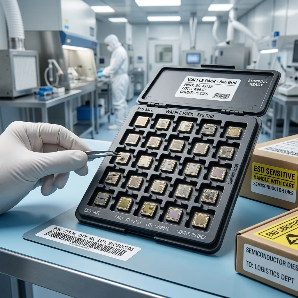
- Mechanical Damage: Silicon is brittle. Improper securing within the carrier media (waffle packs or gel paks) can cause the die to rattle during transit, resulting in edge chipping or micro-cracking.
- Oxidation and Moisture: Exposure to ambient humidity causes the aluminum or copper bond pads to oxidize, severely degrading the reliability of the eventual wire bond or flip-chip bump.
⚡ Sourcing Insight
When sourcing bare die on the independent market, you must demand photographic proof of the original factory packaging (e.g., intact Gel-Pak® or SURF TAPE®). Repackaged bare die without a documented cleanroom chain-of-custody should be considered compromised.
How Should Bare Die Be Packaged and Transported?
To mitigate these risks, the industry relies on highly specialized carrier media. What are the acceptable packaging standards for bare die in 2026?
| Carrier Media Type | Ideal Application | Key Advantage |
|---|---|---|
| Waffle Packs (Chip Trays) | High-volume shipment of standard, robust die sizes. | Cost-effective, automated pick-and-place compatible. Must use anti-static tyvek separator paper. |
| Gel-Paks® (Vacuum Release) | Extremely fragile or highly sensitive RF/optical die. | Die are held securely by a proprietary elastomer gel, preventing mechanical movement. Released via vacuum. |
| Tape and Reel (SURF TAPE) | Mass production, high-speed automated assembly. | Best for very small, robust die (like discrete diodes). |
| Wafer Jars (Film Frame) | Shipping fully sawn wafers still mounted on dicing tape. | Eliminates the need to pick and place individual die before shipping. Requires the end-user to have die-ejector equipment. |
Regardless of the carrier media, all bare die shipments must be vacuum-sealed in Moisture Barrier Bags (MBB) with desiccant and humidity indicator cards (HIC), and transported using specialized, shock-absorbing logistics carriers.
What Should Procurement Demand from Suppliers?
If you are a buyer procuring bare die, you are operating in a high-stakes environment. How do you ensure your supplier won’t ruin the silicon?
- Verify Cleanroom Capabilities: Ensure your supplier or distributor processes all bare die within an ISO Class 5 (Class 100) or better cleanroom environment. Any visual inspection or repacking must occur under laminar flow hoods.
- Demand Strict ESD Protocols: Verify that the supplier adheres to ANSI/ESD S20.20 standards. This includes grounding straps, dissipative flooring, and ionized air blowers in the handling area.
- Require Complete Traceability: Because bare die lack physical markings (silkscreens), maintaining the lot code and wafer batch traceability via the original factory labels is the only way to guarantee authenticity and manage potential yield issues downstream.
Sources:
- SEMI, “SEMI Standards: Guidelines for Bare Die Handling”
- Advanced Packaging Magazine, “The Rise of Chiplet Logistics”
- JEDEC, “J-STD-033: Handling of Moisture/Reflow Sensitive Surface Mount Devices”
- ESDA, “ANSI/ESD S20.20 Standard”
- SupplyICs QA, “Cleanroom Logistics”
[!TIP] Need a reliable partner for sourcing and handling bare die? SupplyICs maintains rigorous QA protocols and partners with certified cleanroom facilities to ensure your highly sensitive silicon arrives in pristine, ready-to-bond condition. Contact us via our Solutions page.
SupplyICs Sourcing Team
Contact Our TeamIndependent Component Specialists
A team of veteran buyers navigating the global spot market. We specialize in locating hard-to-find, shortage, and EOL components. From strict anti-counterfeit verification to cross-reference matching, we provide frontline data to help you secure authentic stock safely.