2026 Semiconductor Fab Construction Timeline and Global Capacity Utilization Analysis
Table of Contents
- 2026 Semiconductor Fab Construction Timeline and Global Capacity Utilization Analysis
- What is the accurate timeline for semiconductor fab construction from cleanroom to commissioning in 2026?
- How do global semiconductor fab capacity utilization rates impact lead times in H2 2026?
- Why should procurement teams track new fab tool install qualifications?
2026 Semiconductor Fab Construction Timeline and Global Capacity Utilization Analysis
⚡ Sourcing Summary
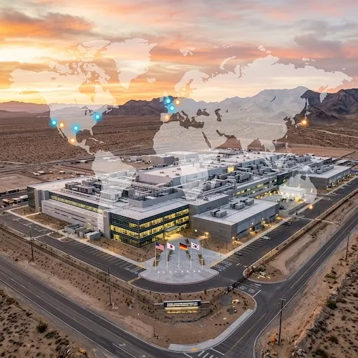
Building a modern semiconductor fab is a massive capital undertaking that consistently requires a 3 to 5-year execution window, making short-term capacity relief highly unlikely. The critical bottlenecks lie not in the shell construction, but in cleanroom commissioning and rigorous tool qualification. With advanced logic fabs demanding **$15 billion to $20 billion** in capital expenditure, supply chain executives must track actual operational data rather than ground-breaking PR announcements. As of mid-2026, global fab capacity utilization for sub-5nm nodes (dominated by **TSMC** and **SMIC**) is sustaining above the critical **90%** threshold. Operating at these high utilization rates eliminates the industry's ability to absorb unexpected shocks, meaning sudden spikes in lead times are virtually guaranteed. Forward-looking procurement teams are actively executing dual-sourcing strategies and securing long-term agreements (LTAs) long before new tools even hit the fab floor.
What is the accurate timeline for semiconductor fab construction from cleanroom to commissioning in 2026?
For procurement managers assessing the time to build a new semiconductor fab, understanding the nuanced phases of construction is more valuable than tracking the initial ground-breaking press release. The industry widely accepts a 3 to 5-year overall timeline, but the critical path for silicon output is heavily weighted toward the backend of this schedule.
In 2026, the timeline breaks down into the following high-level phases:
- Design and Permitting (6-12 months): Environmental impact studies and municipal approvals, heavily influenced by localized regulations (e.g., U.S. CHIPS Act compliance).
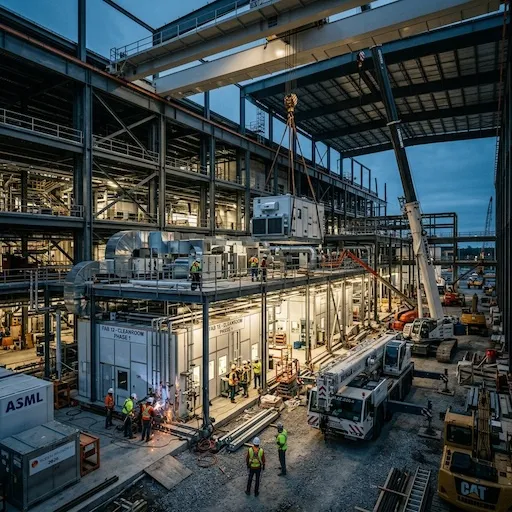
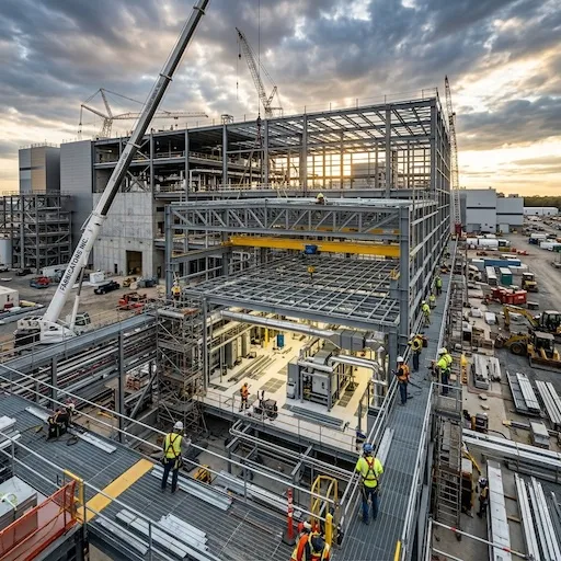
- Base Build / Shell Construction (12-18 months): Erecting the concrete shell, vibration-dampening waffle slabs, and ultra-pure water (UPW) facilities.
- Cleanroom Commissioning (9-12 months): The transition from “dirty” construction to “clean” environment. This phase requires balancing HVAC systems to achieve ISO Class 1 to Class 4 cleanroom standards.
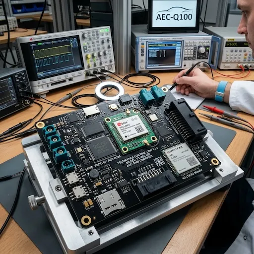
- Tool Install and Qualification (12-15 months): Installing lithography machines (such as ASML EUV scanners), deposition tools, and etching equipment. Each tool requires rigorous calibration.
- Yield Ramp-up (6-12 months): Moving from risk production to high-volume manufacturing (HVM).
Why this matters for your BOM: If a supplier announces a new fab project today, the resulting wafers will not alleviate current allocation issues until at least 2030. Relying on announced capacity rather than commissioned capacity is a fatal flaw in long-term procurement strategy.
Typical Fab Construction Phases (2026 Benchmark)
| Construction Phase | Duration (Months) | Critical Procurement Milestone |
|---|---|---|
| Shell Construction | 12 - 18 | Initial supplier capacity negotiations begin |
| Cleanroom Commissioning | 9 - 12 | LTAs (Long-Term Agreements) locked |
| Tool Qualification | 12 - 15 | Engineering samples available for testing |
| HVM Ramp-up | 6 - 12 | Volume shipments commence |
How do global semiconductor fab capacity utilization rates impact lead times in H2 2026?
The global semiconductor fab capacity utilization in May 2026 serves as the most accurate leading indicator of impending supply chain volatility. Utilization rates measure the percentage of total available wafer capacity that is currently actively processing silicon.
Historically, a utilization rate between 80% and 85% represents an equilibrium market where lead times are stable (typically 12-16 weeks for microcontrollers). However, when utilization surpasses 90%, the dynamic fundamentally shifts. In Q2 2026, driven by the relentless demand for AI accelerators and advanced automotive edge computing, utilization rates at top-tier foundries like TSMC (for 5nm/3nm nodes) and SMIC (for 28nm/14nm mature nodes) have consistently operated above 93%.
At 93% utilization, the foundry loses the ability to seamlessly absorb manufacturing disruptions. A minor equipment failure, a brief power anomaly, or a sudden spike in wafer starts from a Tier-1 hyperscaler results in an immediate backlog. This backlog cascades down the supply chain, extending lead times for standard logic ICs and automotive MCUs from 16 weeks to upwards of 34-40 weeks.
To proactively navigate this:
- Monitor quarterly utilization reports from SIA and Gartner.
- Establish robust Dual Sourcing Strategies to distribute risk across multiple foundries.
Why should procurement teams track new fab tool install qualifications?
The “tool install” phase is the critical threshold where a physical building transforms into a functional silicon factory. During this phase, billions of dollars of equipment—from metrology systems to EUV lithography scanners—are craned into the cleanroom, hooked up to utility mains, and individually calibrated.
Procurement and supply chain executives should track tool install milestones because this phase directly precedes the availability of “engineering samples.” If you are waiting to initiate supplier qualification audits until high-volume manufacturing (HVM) is officially announced, your competitors have already locked in the initial capacity allocations.
By monitoring equipment lead times—which in 2026 often exceed 18 months for specialized etching and deposition tools—buyers can accurately predict exactly when a new fab will actually contribute meaningful supply to the global market, stripping away the optimistic PR spin often associated with facility ground-breaking ceremonies.
References:
- Semiconductor Industry Association (SIA). “2026 Global Wafer Capacity and Fab Construction Report.”
- Gartner. “Supply Chain Risk Management in the Semiconductor Sector (H1 2026).”
- SupplyICs Insights: Navigating Semiconductor Supply Chain Geopolitics in 2026

Sarah Jenkins
LinkedIn ProfileSenior Semiconductor Market Analyst
Sarah Jenkins has over 12 years of experience tracking global wafer allocation, foundry yields, and procurement trends in APAC. She specializes in domestic China fab capacity assessments and geopolitical risk planning for the industrial sector.