Table of Contents
- What Is Driving Bare Die Procurement Growth to $1.44 Billion in 2026?
- When Does It Make Business Sense to Buy Bare Die Instead of Packaged ICs?
- What Are the Real Total Costs of Bare Die Procurement?
- What Is Known Good Die and Why Is It the Single Most Important Procurement Specification?
- How Do You Qualify a Bare Die Supplier — and What Questions Should Procurement Ask?
- What Do the JEDEC Standards Require — and Why Should Procurement Care?
- How Should Procurement Think About Die Banking and Long-Term Bare Die Storage?
- What Are the Most Common Bare Die Procurement Mistakes — and How Do You Avoid Them?
- The Bottom Line
We recently helped an aerospace client who lost a $200,000 bare die shipment due to improper Waffle Pack transfer by an unqualified intermediary. The FPGA dice arrived with edge chipping and oxidation across roughly 40% of the lot—unsalvageable for the wire-bonding process they were designed for. The root cause was not a shipping accident. It was a procurement decision made without understanding the infrastructure required on the receiving end: the buyer had no ISO Class 5 cleanroom, no incoming inspection protocol for bare die, and no relationship with a qualified OSAT partner who could receive and process the silicon. They had simply assumed that buying bare die would be cheaper than packaged FPGAs. The per-die unit cost was indeed lower, but after the yield loss, re-procurement, and project delay, the total cost was nearly triple the packaged alternative.
That experience captures the central tension of bare die procurement in 2026. The market is growing, the technology drivers are real, and the component cost savings can be compelling—but the infrastructure, qualification, and risk-management requirements are orders of magnitude more demanding than packaged IC procurement. Making the right call requires understanding not just the die price but the total cost of ownership, the supply chain architecture, and your organization’s actual readiness to handle unpackaged silicon.
Related Reading: For the operational side of bare die handling—packaging standards, cleanroom protocols, and logistics best practices—see our companion guide: Semiconductor Logistics: How to Manage Bare Die Shipping and Handling in 2026. This article focuses on the procurement decision itself: when bare die makes business sense, how to build the cost model, and what supplier qualifications to demand. For the broader advanced packaging context that drives much of the bare die demand, see: Beyond CoWoS: What Are Your Real Advanced Packaging Options for AI Chips in Late 2026?.
What Is Driving Bare Die Procurement Growth to $1.44 Billion in 2026?
The bare die shipping, handling, processing, and storage market is not growing because more companies decided to buy unpackaged silicon instead of packaged ICs for existing designs. It is growing because the architecture of advanced semiconductor systems has changed in ways that make bare die an input material rather than an optional procurement format. Three structural shifts are responsible. First, chiplet architectures disaggregate what was once a monolithic SoC into multiple smaller die—often fabricated at different process nodes by different foundries—that must be integrated into a single package. Each chiplet begins as a bare die. Second, heterogeneous integration—mixing logic, memory, analog, and RF functions in a 2.5D or 3D package—requires bare die as the fundamental building block; you cannot build a CoWoS or EMIB package from pre-packaged ICs. Third, the advanced packaging capacity build-out itself is a demand driver: every new CoWoS, EMIB, I-Cube, or FoCoS line is a consumption point for bare die, and the combined capacity of these platforms is growing at north of 30% CAGR. The 6.73% CAGR projection to $2.13 billion by 2032 (360iResearch) likely understates reality if advanced packaging capacity growth continues at its current trajectory.
The market data tells a consistent story. The $1.44 billion figure for 2026 represents the services and infrastructure around bare die logistics—the specialized carriers, cleanroom facilities, inspection equipment, storage services, and qualified transportation networks that make bare die supply chains possible. It does not include the value of the silicon itself, which is typically captured under foundry revenue. Mitsubishi Electric’s June 2026 announcement of 5th-generation SiC-MOSFET bare die samples is particularly significant because it extends the bare die conversation beyond the traditional domains of advanced logic and into power semiconductors, where SiC die are increasingly integrated into custom power modules for EV traction inverters, AI data center power supplies, and renewable energy converters. The message for procurement is that bare die is not a niche concern limited to bleeding-edge AI accelerators—it is becoming a mainstream procurement category across multiple semiconductor segments.
📌 Direct Answer: Bare die procurement is growing from $1.35B in 2025 to a projected $1.44B in 2026 because chiplet architectures, heterogeneous integration, and the advanced packaging build-out have transformed bare die from a specialty procurement format into an essential input material. Every advanced package—CoWoS, EMIB, I-Cube, FoCoS—consumes bare die. As advanced packaging capacity grows at 30%+ CAGR, bare die logistics and services grow with it. The Mitsubishi Electric SiC-MOSFET bare die sampling (June 2026) extends this trend into power semiconductors. For procurement teams, the implication is that bare die competency is no longer optional—even if your organization does not buy bare die today, the probability that it will within the next 2-3 years is high and rising.
When Does It Make Business Sense to Buy Bare Die Instead of Packaged ICs?
The decision to buy bare die instead of a packaged IC is not primarily about component cost. It is about whether your product architecture requires unpackaged silicon, and whether your organization has—or can access—the infrastructure to receive, inspect, store, and assemble it without incurring more cost in yield loss and overhead than you save on the component price. We see procurement teams make this evaluation across four dimensions: application architecture, production volume, risk tolerance, and cost structure.
When bare die procurement makes sense: your product uses a multi-chip module, System-in-Package, or 2.5D/3D heterogeneous integration that physically cannot be assembled from packaged ICs. The packaging itself is the product architecture, not an afterthought. Your production volume for the specific die type exceeds roughly 50,000 units annually, amortizing the fixed costs of KGD qualification, cleanroom infrastructure, and specialized logistics. You either operate in-house advanced packaging lines or have a qualified, longstanding relationship with an OSAT partner who handles bare die daily. Your risk tolerance accounts for the reality that bare die assembly yield risk transfers from the component supplier to you—there is no packaged-IC supplier to blame when a wire bond fails. And your total cost model, factoring in all overhead, shows a genuine advantage over the packaged alternative, which happens most often when the packaged version carries a substantial premium for low-volume, high-reliability, or application-specific qualifications that your bare-die-plus-custom-package approach avoids. In every other scenario—standard PCB assembly with single-die packages, volumes below the amortization threshold, lack of cleanroom or OSAT infrastructure, or risk-averse supply chains—packaged ICs remain the lower-total-cost, lower-risk choice.
The following decision matrix summarizes the evaluation across the key dimensions:
| Decision Factor | Favors Bare Die Procurement | Favors Packaged IC Procurement |
|---|---|---|
| Application Architecture | Multi-chip module, SiP, 2.5D/3D heterogeneous integration, chiplet-based design, custom power module | Single-die PCB-mount applications using standard packages (QFN, BGA, SOIC, QFP, LGA) |
| Production Volume | Above ~50,000 units/year per die type—amortizes KGD qualification and cleanroom fixed costs | Below ~10,000 units/year—qualification and infrastructure overhead exceeds component cost savings |
| Packaging Infrastructure | In-house advanced packaging line or qualified OSAT partner with proven bare die handling and ISO Class 5 cleanroom | Standard SMT assembly line; no cleanroom capability beyond standard ESD-protected manufacturing floor |
| Component Cost Sensitivity | Packaged version carries 2-5x premium (low-volume, rad-hard, mil-spec, or application-specific qualified parts) | Packaged version is commodity-priced with minimal premium over bare die plus assembly cost |
| Supply Availability | Packaged IC is allocation-constrained with 52+ week lead times; bare die is available from foundry or die bank | Packaged IC is readily available through authorized distribution with normal lead times |
| Risk Tolerance | Organization accepts assembly yield risk; has in-house failure analysis capability; carries buffer stock for yield loss | Organization requires supplier-guaranteed component-level quality; zero-appetite for assembly yield risk transfer |
| Supply Chain Geography | Assembly site is co-located with or near die source; minimal transit legs between dicing and packaging | Multiple international transit legs; bare die logistics risk (ESD, moisture, contamination) is unacceptably high |
| Product Lifecycle Stage | New product introduction with design optimized for bare die assembly; packaging designed concurrently with silicon | Mature product with proven packaged BOM; redesign to accommodate bare die would cost more than any savings |
The decision is almost never made on die price alone. In our experience working with procurement teams across aerospace, automotive, industrial, and AI sectors, the organizations that succeed with bare die procurement are those that treat it as a supply chain architecture decision—not a component cost optimization exercise. The aerospace client who lost the $200,000 shipment made the classic error: they compared the line-item cost of bare FPGA die against packaged FPGA BGA components, saw a 40% savings, and placed the order without assessing their receiving infrastructure. A proper procurement decision framework would have flagged the absence of cleanroom capability as a hard stop.
What Are the Real Total Costs of Bare Die Procurement?
The per-die price at the foundry or distributor gate is the smallest line item in a bare die procurement cost model. Understanding the full cost stack is essential to making an honest comparison against packaged IC alternatives. Procurement teams that compare only the bare die unit price against the packaged IC unit price are making a decision on roughly half the relevant data.
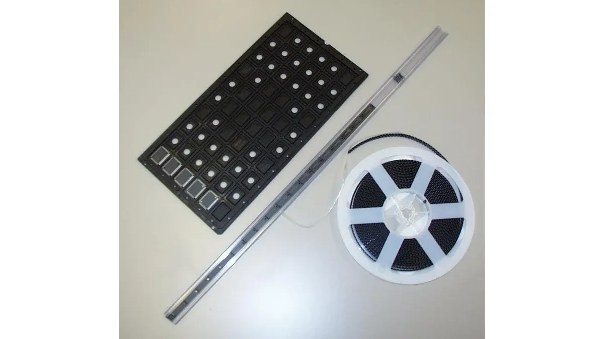
The total cost of bare die procurement comprises at least seven cost categories beyond the die itself. Known Good Die (KGD) qualification—full wafer-level probe testing, burn-in where specified, and statistical yield binning—typically adds 15-30% to the base die cost, but it is non-negotiable: buying bare die without KGD screening transfers the cost of identifying defective die to your assembly line, where the cost of a failed wire-bond or flip-chip attach is orders of magnitude higher than wafer-level rejection. Specialized packaging and shipping materials—Waffle Packs or Gel-Paks, anti-static separator paper, Moisture Barrier Bags with desiccant and humidity indicator cards, and shock-absorbing transport containers—add $0.50 to $3.00 per die depending on die size, fragility, and order volume. Cleanroom receiving, incoming inspection, and storage infrastructure at the buyer’s facility or OSAT partner typically requires ISO Class 5 (Class 100) capability with laminar flow workstations, ionized air, and continuous particle monitoring—capital investment that runs from $500,000 for a basic inspection station to $5 million+ for a full receiving and storage cleanroom. Die banking services for long-term storage of wafers and singulated die—offered by specialists like Micross—cost approximately $500 to $2,000 per month for a standard wafer lot, with nitrogen-purged cabinet storage and periodic outgoing inspection. Assembly yield risk is the hardest cost to quantify but often the most significant: unlike packaged IC procurement where the component supplier guarantees functional parts, bare die procurement means you own the yield from wafer saw through final package test, and a 2-5% assembly yield loss on a high-value die can erase the component cost savings for the entire lot. Logistics insurance premiums for bare die shipments are typically 2-3x the packaged IC equivalent due to the fragility and contamination sensitivity of unpackaged silicon. And supplier qualification costs—including on-site audits of cleanroom facilities, test capability verification, and ongoing quality monitoring—add $20,000-50,000 for initial qualification and $10,000-20,000 annually for each bare die supplier relationship.
When we build total cost models for clients evaluating a bare die versus packaged IC decision, the all-in bare die procurement cost typically runs 25-50% above the wafer-level die price. The question is whether the packaged IC alternative carries an even higher premium. In our experience, bare die procurement wins on total cost in two scenarios: when the packaged IC carries a substantial specialty premium (radiation-hardened, military-temperature-range, or aerospace-qualified parts where the packaged version may cost 3-10x the commercial equivalent) and when the product architecture genuinely requires bare die and the comparison is not bare die versus packaged IC but bare die versus “no viable packaged alternative exists.”
What Is Known Good Die and Why Is It the Single Most Important Procurement Specification?
We have seen procurement teams negotiate aggressively on bare die unit pricing while treating KGD qualification as an afterthought. This is the most expensive mistake in bare die procurement. Known Good Die is a test and qualification methodology that verifies each individual bare die meets its electrical specifications before it leaves the supplier—essentially performing the same screening function that final test does for a packaged IC, but at the wafer level. Without KGD, you are buying statistical probability rather than functional certainty.
KGD qualification exists because bare die lack the physical protection and standardized test interfaces of packaged components. In a packaged IC flow, the supplier performs final electrical test after packaging—probing the device through its package pins or balls, running it through burn-in to precipitate early-life failures, and shipping only the units that pass. The packaging process itself creates a filter: defective die that would fail at wafer probe are caught before they reach a customer’s board. Bare die procurement removes this filter. The die are singulated from the wafer, placed in carrier media, and shipped without any further electrical verification beyond what the foundry performed at wafer sort—and the correlation between wafer sort results and final packaged-part performance is imperfect, especially for high-speed, RF, or mixed-signal devices where the probe environment differs significantly from the intended application environment. KGD bridges this gap by adding test steps—extended wafer probe at temperature, burn-in on temporary carriers, and sometimes Known Good Die-level functional test—that approach the confidence level of packaged IC final test. The cost adder (15-30%) is insurance against assembly-line failures where a defective die is discovered only after it has been wire-bonded or flip-chip-attached into an expensive substrate. We consider KGD the single non-negotiable procurement specification for any bare die that will be assembled into a multi-chip module, SiP, or other advanced package where rework is difficult or impossible.
Die banking services like those offered by Micross add a related dimension to the KGD equation. Long-term storage of wafers and singulated bare die—sometimes spanning years, as when a defense program procures a lifetime buy of a soon-to-be-discontinued die—requires environmental controls that preserve the bond pad integrity and prevent the gradual degradation that can turn KGD into “no longer known good die” over time. Nitrogen-purged storage cabinets, periodic outgoing inspection, and controlled humidity environments are the minimum. Procurement teams planning lifetime buys of bare die should factor die banking costs into their total cost model from the start, not discover them when the first stored lot fails incoming inspection three years into the program.
How Do You Qualify a Bare Die Supplier — and What Questions Should Procurement Ask?
Supplier qualification for bare die is fundamentally different from packaged IC supplier qualification because the risk surface is different. With packaged ICs, the supplier’s packaging process is their problem—if the mold compound delaminates or the wire bonds fail, you return the parts. With bare die, the supplier’s handling, storage, testing, and packaging processes become your problem downstream. A qualification gap at the supplier translates directly into assembly yield loss on your line.
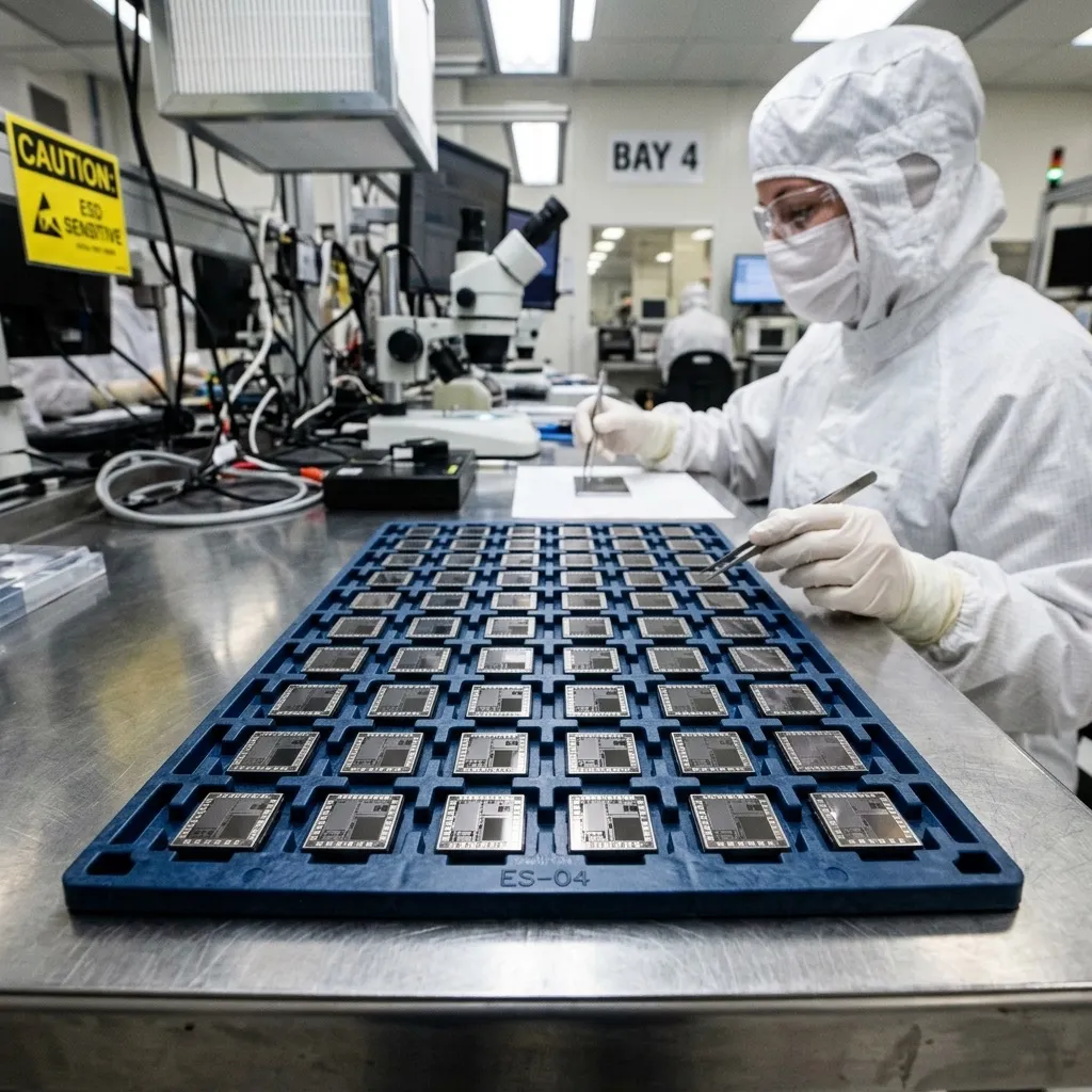
A bare die supplier qualification must cover six domains. First, cleanroom certification and practice: the supplier must operate a certified ISO Class 5 (Class 100) or better cleanroom for all bare die handling operations, with documented environmental monitoring data—particle counts, temperature, and humidity logs—available for audit. A certificate on the wall is insufficient; you need to see the data. Second, ESD control: the supplier’s ESD program must comply with ANSI/ESD S20.20, and this means more than wrist straps at workstations. It requires dissipative flooring, continuous monitoring of grounding systems, ionized air blowers at every handling station, and verification that carrier media (Waffle Packs, Gel-Paks) are themselves static-dissipative and properly conditioned. Third, KGD test capability and data transparency: the supplier must provide full wafer probe maps, statistical process control data by wafer lot, and correlation studies between wafer-level test results and packaged-part performance for the specific device type. If the supplier cannot or will not share probe data, assume they are not performing adequate screening. Fourth, traceability infrastructure: because bare die have no package markings, traceability depends entirely on the integrity of the supplier’s lot-control and labeling systems. Every die must be traceable to its wafer lot, wafer number, and wafer-map coordinates. The supplier must demonstrate that this traceability survives the singulation, pick-and-place into carrier media, and shipping processes intact. Fifth, packaging and shipping protocol: the supplier must package bare die in accordance with JEDEC J-STD-020 (moisture sensitivity classification) and J-STD-033 (handling, packing, and shipping of moisture-sensitive devices). This means vacuum-sealed Moisture Barrier Bags with fresh desiccant and humidity indicator cards, appropriate carrier media (Waffle Pack, Gel-Pak, or tape-and-reel per the die specifications from Toshiba and other manufacturers), and shock-absorbing outer packaging rated for the transportation mode. Sixth, financial stability and business continuity: bare die supply sources are specialized and not easily replaced. The supplier’s financial health, succession planning, and disaster recovery capabilities should be part of the qualification assessment. A supplier who is the sole qualified source for your die and goes out of business creates a requalification problem that can take 6-12 months to resolve.
The supplier conversation should include specific, technical questions. “What is your cleanroom classification and when was it last re-certified?” “Show me your particle count logs for the past 90 days.” “Describe your wafer-probe-to-carrier-media transfer process step by step.” “What is your procedure when a HIC shows humidity excursion upon receiving inspection?” “How do you maintain traceability from wafer lot to individual Waffle Pack cell?” “What is your corrective action process when a customer reports die damage upon receipt?” Suppliers who answer these questions with documented processes, data, and specific examples demonstrate the operational maturity required for bare die supply. Suppliers who answer with assurances rather than evidence are not ready.
What Do the JEDEC Standards Require — and Why Should Procurement Care?
JEDEC standards are technical documents, but procurement teams should understand their operational implications because they define the minimum acceptable practices that protect your bare die investment. Two standards are central: J-STD-020, which classifies devices by their moisture sensitivity level (MSL), and J-STD-033, which specifies the handling, packing, and shipping requirements for moisture-sensitive surface-mount devices. Although these standards were originally written with packaged components in mind, their principles apply with even greater force to bare die because unpackaged silicon has zero moisture barrier.
J-STD-020 defines moisture sensitivity levels from MSL 1 (unlimited floor life) to MSL 6 (mandatory bake before use). Bare die are effectively MSL 6 by default—any exposure to ambient humidity risks oxidation of aluminum or copper bond pads, which degrades wire-bond pull strength and flip-chip bump reliability. J-STD-033 specifies the protective measures required for each MSL: Moisture Barrier Bags with a water vapor transmission rate below 0.02 g/m²/24 hours, desiccant sufficient to maintain less than 10% relative humidity inside the sealed bag for the expected shelf life, and a Humidity Indicator Card that provides a visual confirmation that the bag’s interior environment has remained dry. The standard also specifies the bake-out procedure if the HIC shows a humidity excursion: typically 125 degrees Celsius for 24-48 hours for bare die, though the exact profile must be validated for the specific die metallization to avoid intermetallic growth at the bond pad interface. For procurement, the practical implication is straightforward: every bare die shipment must arrive in an intact, undamaged MBB with a HIC showing the dry state, and your receiving process must include verification of bag integrity and HIC status before the shipment is accepted. A shipment with a breached MBB or a tripped HIC should be rejected or, at minimum, quarantined for bake-out and re-inspection before use.
Toshiba’s published semiconductor handling precautions provide a useful industry reference point. Their guidelines emphasize that bare die should be handled only at ESD-protected workstations with grounded operators, that carrier media should never be opened outside a cleanroom environment, and that die should be stored in nitrogen-purged cabinets when not in active processing. These are not aspirational best practices—they are the minimum necessary to prevent the failure mechanisms (ESD damage, contamination, oxidation) that silently destroy bare die yield. Procurement teams should include adherence to these standards as explicit requirements in their supplier contracts and quality agreements, with defined consequences for non-compliance including rejection rights and cost-recovery provisions for yield loss attributable to improper handling.
How Should Procurement Think About Die Banking and Long-Term Bare Die Storage?
Die banking—the practice of purchasing and storing wafers or singulated bare die for future use—is a specialized procurement strategy that addresses a specific problem: components that are essential to a long-lifecycle product but at risk of obsolescence. It is most common in defense, aerospace, medical device, and industrial control applications where product lifecycles span 15-30 years but semiconductor fabrication cycles often end after 5-7 years. The strategy is straightforward in concept: buy the silicon while the foundry is still running the process, store it under controlled conditions, and draw from the bank as needed over the product lifecycle. Execution is considerably more complex.
Die banking makes sense when three conditions are met: the bare die in question has no packaged equivalent available (or the packaged version is also going obsolete), the end product’s lifecycle exceeds the semiconductor’s forecasted production window by at least 5 years, and the organization has access to—or contracts for—professional die storage services with documented environmental controls and periodic outgoing quality inspection. Services like Micross provide nitrogen-purged, humidity-controlled storage environments specifically designed for long-term bare die preservation, with monitoring and reporting that satisfies the traceability requirements of regulated industries. The cost—$500 to $2,000 per month per wafer lot—is modest relative to the cost of a line-down situation on a multi-decade defense or medical program. However, die banking is not “buy and forget.” Even under optimal storage conditions, bare die degrade over time. Aluminum bond pads oxidize slowly even in nitrogen environments if trace oxygen or moisture is present. Gold bond pads are more chemically inert but introduce gold-aluminum intermetallic concerns if the assembly process uses aluminum wire. Solder bumps on flip-chip die can experience intermetallic growth that changes the bump mechanical properties. The practical shelf life of properly stored bare die is typically 5-10 years for aluminum-pad devices and 10-15+ years for gold-pad devices, but this must be validated per device type and storage protocol. Procurement teams planning die banking strategies should include periodic outgoing sampling and bondability testing in their storage contracts, with defined acceptance criteria and a trigger plan for when a banked lot no longer meets assembly requirements.
A related strategy that we have seen deployed effectively is wafer banking—purchasing complete, un-diced wafers and storing them until die are needed, at which point the wafers are diced, inspected, and the die singulated. Wafer banking has the advantage of protecting the die surface throughout storage (the un-diced wafer’s passivation layer provides some environmental protection that singulated die lack) but requires access to dicing capability at the time of withdrawal, which adds a processing step and cost. The choice between die banking and wafer banking depends on whether your assembly partner has dicing capability, the die size and wafer diameter, and the expected withdrawal pattern (singulated die are easier to draw in small quantities; wafers make sense when you expect to consume an entire wafer’s worth of die at a time).
What Are the Most Common Bare Die Procurement Mistakes — and How Do You Avoid Them?
The lessons in this article are drawn from real procurement outcomes, and the pattern of mistakes is consistent enough across industries that it is worth cataloging explicitly. These are the failure modes we see repeatedly when organizations venture into bare die procurement without adequate preparation.
The five most common and costly bare die procurement mistakes are: (1) Comparing die price to packaged IC price without building the total cost model—this produces decisions based on roughly half the relevant cost data and almost always underestimates the true cost of bare die procurement by 25-50%. (2) Skipping or under-specifying KGD qualification—this is the single most expensive error in dollar terms, because the cost of discovering a defective die after it has been assembled into a substrate (wire-bonded, underfilled, or flip-chip-attached) is 10-100x the cost of rejecting it at wafer probe. (3) Procuring bare die without verifying receiving infrastructure—we have seen multiple cases where bare die arrived at a standard SMT factory with no cleanroom, were opened in an uncontrolled environment, and were functionally destroyed before they reached the assembly line. (4) Assuming traceability will be maintained without explicit requirements—bare die have no markings; if the supplier’s lot-control system fails and dice from different wafers or lots are mixed, there is no way to untangle them and the entire shipment must be scrapped if lot-level traceability is a requirement. (5) Treating bare die procurement as a sourcing event rather than a supply chain architecture decision—the organizations that succeed with bare die procurement are those that invest in long-term supplier relationships, cleanroom infrastructure, and assembly partnerships, not those that treat it as a spot-buy opportunity when packaged parts are on allocation.
The avoidance strategy for each of these mistakes is straightforward but requires organizational discipline. Build the total cost model before making the procurement decision. Specify KGD and audit the supplier’s test data, not just their certificate. Verify that the receiving site has the cleanroom, ESD, and inspection equipment specified in the handling protocol before the first shipment arrives. Write traceability requirements into the procurement contract with defined consequences for lot-mixing events. And approach bare die procurement as a strategic supply chain investment with a multi-year horizon, not a tactical response to a short-term packaged IC shortage. The $200,000 loss our aerospace client experienced was the product of all five mistakes compounding—and it is entirely avoidable with the right procurement framework in place.
Need help evaluating whether bare die procurement fits your product architecture and supply chain? SupplyICs’ engineering and procurement teams have guided clients across aerospace, defense, medical, industrial, and AI sectors through bare die sourcing decisions—from initial cost modeling through supplier qualification and logistics setup. Upload your BOM for a confidential bare die procurement assessment, or explore our sourcing solutions to see how we manage the specialized logistics, quality assurance, and supplier relationships that bare die procurement demands.
The Bottom Line
Bare die procurement in 2026 is not a niche concern and not a universal solution. It is a procurement decision that makes sense in specific, well-defined circumstances—when your product architecture demands unpackaged silicon, your volume amortizes the infrastructure, and your organization has (or contracts for) the cleanroom, test, and storage capabilities that bare die require. The $1.44 billion market (360iResearch, 2026) and 6.73% CAGR reflect genuine structural demand growth driven by chiplet architectures, heterogeneous integration, and the advanced packaging build-out. Mitsubishi Electric’s SiC-MOSFET bare die sampling extends the conversation into power semiconductors. Die banking services are maturing. The tools and infrastructure exist.
What remains is the organizational discipline to make the decision correctly: build the total cost model, specify and verify KGD, qualify suppliers against the full set of bare-die-specific requirements, and treat bare die procurement as a strategic supply chain investment rather than a tactical cost play. The organizations that do this systematically will capture the architectural and cost advantages that bare die procurement can offer. The organizations that skip the framework and compare die price to packaged IC price will lose money—sometimes a lot of it—and learn the lessons the hard way.
Frequently Asked Questions (FAQ)
When does buying bare die make more business sense than buying packaged ICs?
Bare die procurement makes sense when three conditions align: (1) your product requires custom advanced packaging such as a multi-chip module, System-in-Package, or 2.5D/3D heterogeneous integration that cannot use off-the-shelf packaged components; (2) your production volume justifies the additional logistics, handling, and qualification overhead—typically above 50,000 units per year for a given die type; and (3) you have either in-house advanced packaging capability or a qualified OSAT partner with proven bare die handling protocols. For standard PCB-mount applications using single-die packages (QFN, BGA, SOIC), packaged ICs remain the lower-risk, lower-total-cost option in nearly all cases.
What are the hidden costs of bare die procurement that most buyers underestimate?
The most commonly underestimated costs are: Known Good Die (KGD) qualification—full probe and burn-in at wafer level can add 15-30% to the die unit cost; specialized packaging and shipping—Waffle Packs, Gel-Paks, Moisture Barrier Bags, desiccant, and humidity indicator cards add $0.50-3.00 per die depending on volume and fragility; cleanroom receiving and inspection infrastructure at the buyer's facility or OSAT partner; die banking fees for long-term wafer and die storage (approximately $500-2,000/month for a standard wafer lot at services like Micross); and the yield-loss risk—unlike packaged ICs where the supplier absorbs packaging-related failures, bare die procurement transfers assembly yield risk to the buyer. Factoring all of these in, the all-in cost of bare die procurement is typically 25-50% higher than the wafer-level die price alone.
How do I qualify a bare die supplier and what should a procurement checklist include?
A bare die supplier qualification checklist must cover: (1) cleanroom certification—ISO Class 5 (Class 100) or better with documented environmental monitoring; (2) ESD control program compliant with ANSI/ESD S20.20 including grounding, ionizers, and dissipative surfaces; (3) Known Good Die test capability—the supplier must provide probe test data, burn-in results where applicable, and a statistical yield report by wafer lot; (4) traceability infrastructure—because bare die lack package markings, full lot-code and wafer-map traceability from foundry through shipment is non-negotiable; (5) packaging protocol consistent with JEDEC J-STD-020 and J-STD-033, including vacuum-sealed Moisture Barrier Bags with desiccant and HIC; and (6) financial stability and business continuity planning, given the specialized nature of bare die supply and the difficulty of qualifying alternative sources mid-production.