Table of Contents
- What DDR4 geometry must match before a replacement can boot?
- How do you compare DDR4 timing at the actual operating clock?
- Review refresh and temperature operation
- Test retained-power and reset paths
- Why must DDR4 training be repeated after a component substitution?
- Control firmware and part approval together
DDR4 substitution is a controller-and-board qualification, not a capacity match. Density, organization, bank structure, rank topology, package, speed bin, and refresh behavior all influence initialization and timing.
Begin by decoding the existing memory configuration. The approved alternate must fit both the schematic wiring and the memory controller’s supported geometry before signal-integrity testing has value.
What DDR4 geometry must match before a replacement can boot?
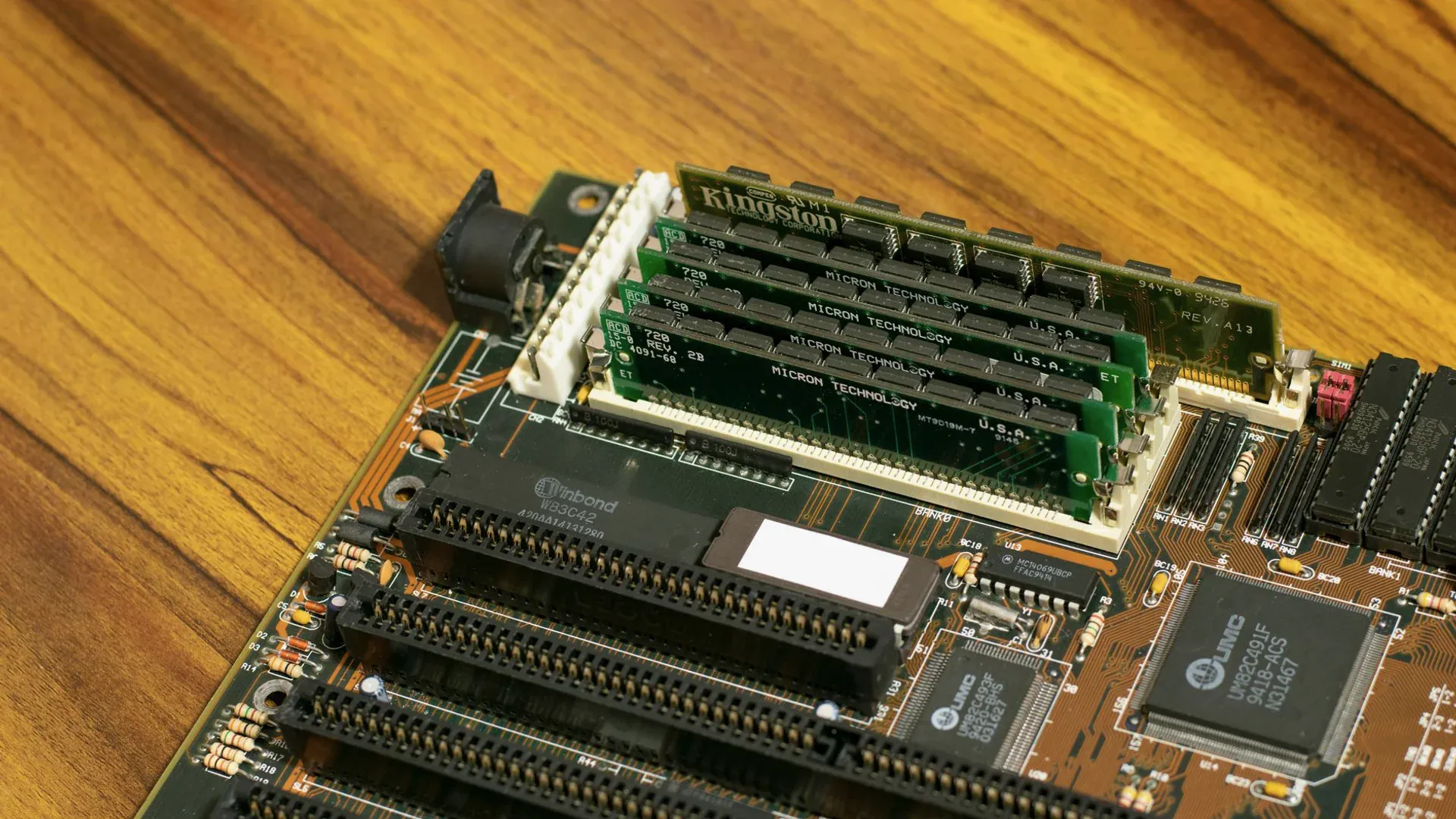
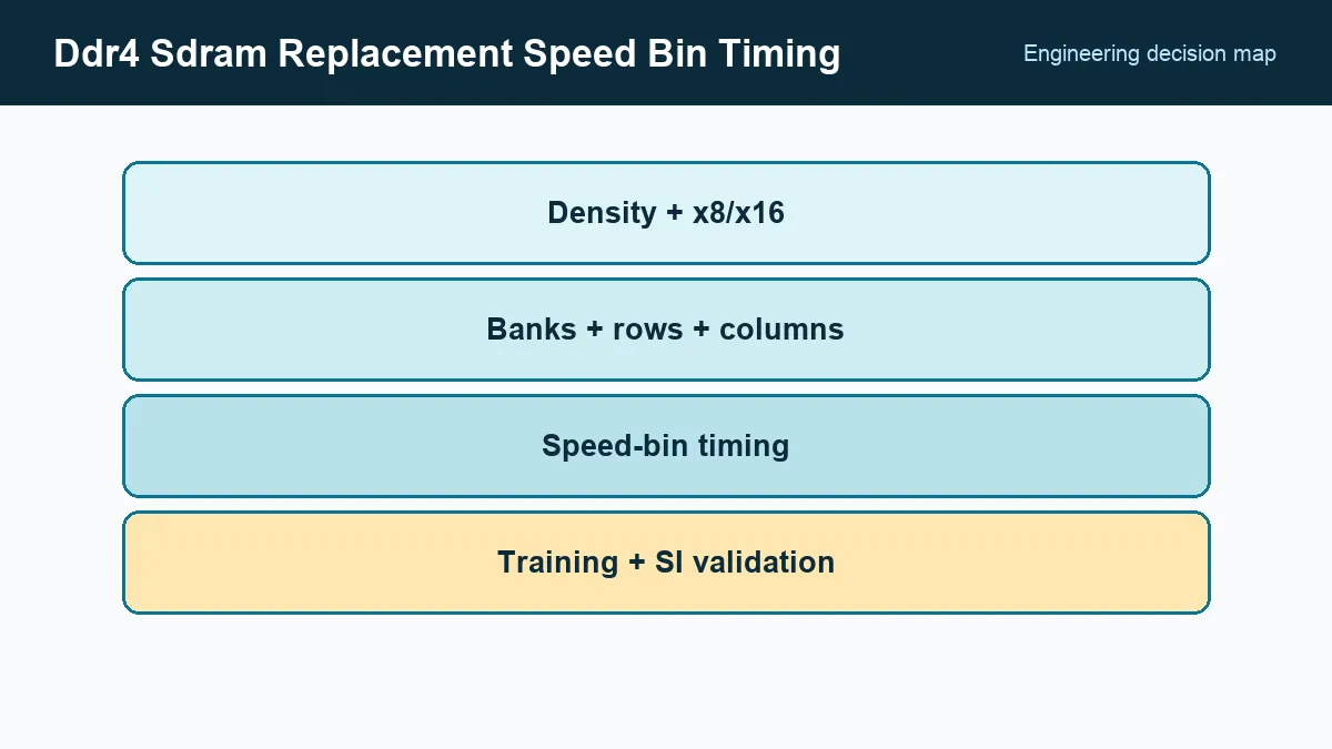
A DDR4 replacement must use a density, data width, bank structure, rank arrangement, and address map supported by both the memory controller and the board wiring. Matching total capacity is insufficient; record the package ball map, die stack, and temperature grade alongside the controller’s data-width and ECC-lane configuration.
A 16 Gb x16 part and a 16 Gb x8 part have the same density but present different data width and addressing. The controller may support only certain row/column combinations or total ranks. Firmware tables often encode these assumptions.
Micron’s DDR4 SDRAM product information, accessed September 24, 2026, distinguishes component densities, organizations, and speed options. Use the full data sheet and ordering decoder for the candidate rather than a distributor’s abbreviated attribute list.
How do you compare DDR4 timing at the actual operating clock?
Compare the original and candidate DDR4 devices at the board’s actual clock period, supported CAS latency, voltage, and temperature. Check tCK, tRCD, tRP, tRAS, tRC, tRFC, tFAW, tRRD, write recovery, command timing, and refresh requirements; the marketed data rate alone does not define a compatible timing set.
A higher speed bin may operate at a lower rate, but firmware must select a CAS latency and mode-register combination supported by that bin at the actual tCK. Timing values expressed in nanoseconds can translate into different cycle counts. Round in the safe direction according to controller rules.
Samsung’s 8 Gb DDR4 x16 specification, accessed September 24, 2026, shows how timing tables, organization, and package information coexist in a component data sheet. Repeat that field-by-field comparison for both original and alternate.
Review refresh and temperature operation
Refresh-cycle time increases with density, and refresh rate can change at elevated temperature. Ensure the controller can issue the required refresh mode and that firmware detects or assumes temperature correctly. Compare self-refresh, auto self-refresh, and temperature-controlled refresh features used in low-power states.
Test retained-power and reset paths
If the product retains memory through suspend, test entry, steady retention, and exit at temperature. Initialization after a warm reset can differ from a complete power removal, so include both paths. Exercise reset with clocks stopped, rails retained, and rails ramped in every state supported by the controller documentation.
Capture whether firmware retrains or reuses stored parameters. Reusing data obtained for another memory ordering code can conceal a marginal alternate during development and fail after process or temperature variation.
Why must DDR4 training be repeated after a component substitution?
A DDR4 substitute can change input capacitance, output drive, or package parasitics enough to move the data eye despite an identical pinout. Repeat the controller’s write leveling, read-gate training, data-eye centering, and Vref training as applicable, and retain measured margins rather than only a boot pass.
Test multiple boards and memory lots across voltage and temperature, repeated cold boots, warm resets, and supported frequencies. Exercise data patterns that expose coupling and simultaneous switching. If the controller stores trained values, verify the reuse rules after component substitution.
Review termination, on-die termination, drive strength, Vref range, and PCB topology. Simulation models should match the package and die option when high-speed margin is narrow.
Control firmware and part approval together
The qualification record should include the schematic population, controller configuration, initialization source, timing calculations, mode-register values, training plots or logs, stress-test coverage, and failure thresholds. Keep the boot firmware hash with the test evidence.
The purchasing specification should lock manufacturer, ordering code, geometry, package, speed grade, temperature grade, refresh constraints, and approved firmware baseline. When a supplier proposes a faster or denser part, engineering can then see whether it fits the established controller contract instead of assuming that downward clock compatibility resolves every difference.
Frequently Asked Questions (FAQ)
Can a faster DDR4 speed grade replace a slower one?
Often it supports lower clock rates, but the host must program a valid timing set for that device and geometry. Refresh, mode-register support, package loading, and training margin still require verification.
Why does x8 versus x16 DDR4 organization matter?
Organization changes data width per component, bank structure, controller configuration, routing, ECC construction, and the number of devices needed for a channel. Equal total density does not make the geometries interchangeable.
Is passing a memory test at room temperature sufficient?
No. Training and timing margin should be tested across supported frequency, voltage, temperature, board population, and representative traffic patterns, including repeated cold and warm boots.