Table of Contents
- How Has Wafer Shipping Become a Strategic Procurement Function?
- 1. The Value Density Explosion
- 2. The Chiplet-Driven Proliferation of Bare Die Shipments
- 3. Geopolitical Fragmentation of Fab Locations
- Wafer Carrier Technology: A Procurement Selection Guide
- FOUP (Front Opening Unified Pod)
- FOSB (Front Opening Shipping Box)
- 200mm SMIF Pods and Open Cassettes
- Emerging: 450mm and Panel-Level Carriers
- What Makes a Qualified Wafer Logistics Provider?
- Environmental Monitoring Infrastructure
- Cleanroom Capability for Transshipment
- ESD Control Program
- Carrier Procurement Best Practices
- 1. Standardize on a Single Carrier Ecosystem
- 2. Carrier Pooling vs. Owned Inventory
- 3. Track Carrier Lifecycle Usage
When a 300mm wafer carrying $500,000 worth of 3nm logic dies leaves TSMC’s Fab 18 in Tainan for a packaging facility in Arizona, it travels approximately 12,000 kilometers. It crosses multiple climate zones, changes hands at least six times, and experiences vibration, temperature cycling, and pressure changes. The wafer carrier—the seemingly mundane plastic box that holds the wafer—is the only thing standing between that half-million-dollar asset and catastrophic loss.
In 2026, wafer shipping and handling has become a strategic procurement discipline. The decisions procurement teams make about carriers, logistics providers, and handling protocols have direct P&L impact. A single mis-specified carrier can cause a wafer breakage event that wipes out weeks of production margin.
How Has Wafer Shipping Become a Strategic Procurement Function?
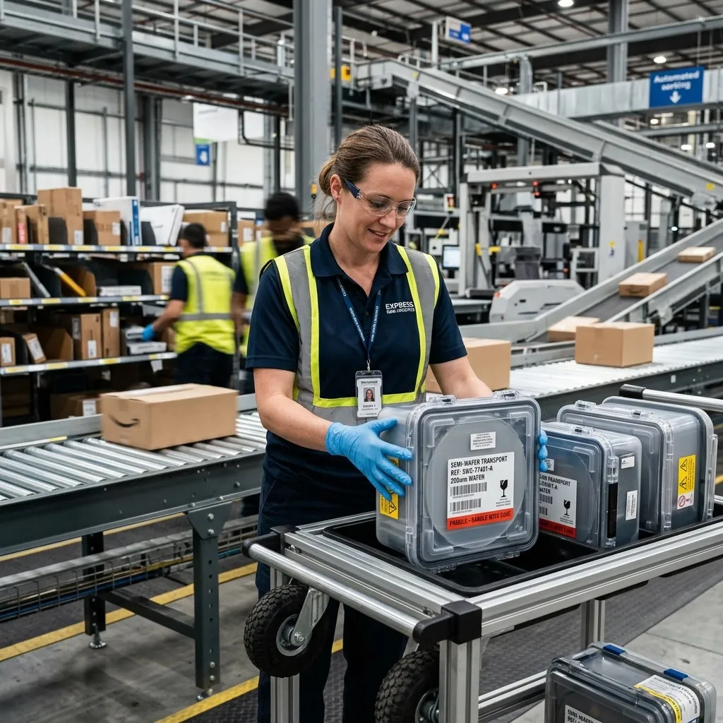
Three structural shifts have elevated wafer logistics from tactical execution to strategic risk management:
1. The Value Density Explosion
A 300mm wafer of 28nm microcontroller dies in 2020 was worth roughly $20,000–40,000. A 300mm wafer of 3nm AI accelerator dies in 2026 is worth $300,000–500,000. The shipping and handling cost as a percentage of cargo value has actually decreased—but the absolute cost of failure has increased by an order of magnitude.
This changes the procurement calculus. When a shipment is worth $50,000, adding $500 of enhanced packaging to reduce damage risk from 2% to 0.2% has a positive expected value of $900 per shipment. When a shipment is worth $500,000, the same improvement has an expected value of $9,000—and the enhanced packaging becomes non-negotiable.
2. The Chiplet-Driven Proliferation of Bare Die Shipments
Multi-chip module architectures require bare die from multiple foundries to converge at a single OSAT location. This creates a hub-and-spoke logistics model where wafer and die shipments converge from Taiwan, South Korea, the United States, and Europe, each following different carrier standards and environmental requirements.
The procurement challenge: standardizing carrier formats across a multi-vendor, multi-geography supply chain without imposing costs that erase the economic benefits of chiplet disaggregation.
3. Geopolitical Fragmentation of Fab Locations
As CHIPS Act-funded fabs come online in the United States, Europe, Japan, and India, the semiconductor supply chain is physically dispersing. A chip designed in Silicon Valley may be fabricated in Arizona, packaged in Malaysia, and tested in the Philippines—a logistics chain that did not exist five years ago. Each new node in the chain adds handling steps, and each handling step adds damage risk.
Wafer Carrier Technology: A Procurement Selection Guide
The wafer carrier is the fundamental unit of wafer logistics. Selecting the right carrier for your process node, transport distance, and volume is the highest-leverage procurement decision in wafer shipping.
FOUP (Front Opening Unified Pod)
- Application: Intra-fab automated transport (300mm)
- Environment: Internal Class 1 cleanroom maintained by nitrogen purge
- Interface: Automated load port (SEMI E15.1 standard)
- Procurement Classification: Capital equipment (5–7 year depreciation)
- Key Suppliers: Entegris, Shin-Etsu Polymer, Miraial, Gudeng Precision
- Selection Criteria: Particle generation rate (<0.1 particles/cm² per cycle), outgassing specification, RFID compatibility, AMHS interoperability
FOSB (Front Opening Shipping Box)
- Application: Inter-fab and intercontinental transport (300mm)
- Environment: Sealed with desiccant, often nitrogen backfilled
- Interface: Manual or automated unpacking at receiving fab
- Procurement Classification: Consumable or reusable (3–10 trips typical)
- Key Suppliers: Entegris, Shin-Etsu Polymer, Miraial, 3S Korea
- Selection Criteria: Shock/vibration isolation, seal integrity over temperature cycling (-20°C to +60°C range), stacking strength for air and sea freight, RFID/GPS tracking compatibility
200mm SMIF Pods and Open Cassettes
- Application: 200mm wafer transport (still ~30% of global wafer production)
- Procurement Note: The 200mm carrier market is mature but facing supply constraints as manufacturers shift production capacity to 300mm tooling. Procurement teams should maintain 3–6 months of carrier inventory buffer, as lead times for replacement 200mm carriers have extended from 4–6 weeks to 12–16 weeks in 2026.
Emerging: 450mm and Panel-Level Carriers
For 450mm wafers (limited production) and panel-level packaging substrates (510 × 515 mm glass or organic panels), carrier standards are still evolving. Procurement teams involved in these emerging formats should participate in SEMI standards committees to influence carrier specifications before they are locked.
What Makes a Qualified Wafer Logistics Provider?

Environmental Monitoring Infrastructure
A qualified wafer logistics provider should offer:
- Real-time GPS tracking with geofencing alerts
- Temperature and humidity data logging at 5-minute minimum intervals
- Shock and vibration monitoring (tri-axial accelerometer, >200 Hz sampling)
- Tilt and tip detection for carriers that must remain upright
The data from these sensors should be available to the procurement team in real time, not provided as a post-shipment report. If a shipment exceeds temperature limits, the procurement team needs to know immediately—not three days after the wafer has been processed and latent damage has been baked into finished product.
Cleanroom Capability for Transshipment
If a wafer shipment requires intermediate handling—repackaging, inspection, or consolidation—the logistics provider must have ISO Class 5–7 cleanroom capability at the transshipment point. Wafer-level handling requires ISO Class 5 (Class 100) as a minimum; die-level handling in carrier media can tolerate ISO Class 7 (Class 10,000).
ESD Control Program
The provider’s ESD control program should be audited to ANSI/ESD S20.20, with specific verification of:
- Grounded flooring and work surfaces in all wafer-handling areas
- Personnel grounding tested at shift start (wrist strap < 3.5 × 10⁷ Ω to ground)
- Ionization over workstations where wafers are exposed
- Packaging materials compliant with ANSI/ESD S541 (surface resistance 10⁴–10¹¹ Ω)
Carrier Procurement Best Practices
1. Standardize on a Single Carrier Ecosystem
Procurement teams managing wafer shipments across multiple fabs and OSATs should drive standardization on a single carrier ecosystem (e.g., Entegris 300mm FOUP/FOSB platform or Shin-Etsu equivalent). This reduces the training burden on handling personnel, simplifies spare parts inventory, and improves carrier utilization through shared pools.
2. Carrier Pooling vs. Owned Inventory
For high-volume wafer flows (1,000+ wafers/month), carrier pooling services from Entegris or Miraial can reduce total carrier cost by 20–30% compared to owned-and-managed inventory. The pooling provider manages cleaning, inspection, repair, and replacement—converting a Capex + Opex model to a per-use fee.
For lower volumes or specialized carriers (e.g., for thinned wafers below 100 μm), owned inventory typically provides better cost economics and supply assurance.
3. Track Carrier Lifecycle Usage
Each FOSB or wafer cassette has a finite service life measured in clean/use cycles. Exceeding the rated cycle count increases particle generation and seal degradation risk. Implement RFID-based cycle counting to track carrier usage and trigger preventive replacement before failure.
Managing wafer and IC logistics across a multi-fab, multi-geography supply chain? SupplyICs provides logistics coordination, carrier format consulting, and qualified provider selection for semiconductor shipments. Contact our supply chain team for a wafer logistics assessment.
Frequently Asked Questions (FAQ)
What is the difference between a FOUP and a FOSB for wafer transport?
A FOUP (Front Opening Unified Pod) is a sealed, mechanically standardized container used for transporting 300mm wafers within a fab's automated material handling system (AMHS). It maintains an internal nitrogen-purged, Class 1 cleanroom environment and interfaces with automated load ports. A FOSB (Front Opening Shipping Box) is designed for inter-fab transport—it provides similar contamination protection but is ruggedized for truck, air, and sea freight with shock and vibration isolation. For 200mm wafers, SMIF (Standard Mechanical Interface) pods serve the FOUP function, and 200mm shipping cassettes serve the FOSB function. The critical procurement distinction: FOUPs are fab Capex (capital equipment, depreciated over 5–7 years), while FOSBs are typically classified as consumables in the logistics budget.
How do I select the right wafer carrier for my process node and transport distance?
Select wafer carriers based on three parameters: (1) Wafer diameter—300mm requires FOUP/FOSB with automated handling interfaces; 200mm uses SMIF pods or open cassettes; (2) Transport distance—intra-fab uses FOUP/SMIF; inter-fab (domestic) uses FOSB; intercontinental uses vacuum-sealed FOSB with active shock monitoring; (3) Process node sensitivity—sub-7nm nodes require nitrogen-purged carriers with <0.1μm particle filtration; mature nodes (>28nm) can use standard sealed carriers. For 450mm wafers (emerging), carriers are in early standardization and commanded premium pricing as of 2026. The wafer carrier market is projected at USD 0.73 billion in 2026, growing at 6.14% CAGR to USD 1.24 billion by 2035 (Business Research Insights, July 2026).
What are the most common causes of wafer damage during shipping and how can procurement prevent them?
The top three causes: (1) Vibration-induced micro-cracking from inadequate shock isolation (accounts for ~40% of shipping damage claims); (2) Particulate contamination from outgassing carrier materials or breached seals (accounts for ~30%); and (3) ESD damage from non-conductive carriers generating triboelectric charge during transit (accounts for ~20%). Prevention starts at procurement: specify ESD-compliant carrier materials (surface resistivity 10⁴–10¹¹ Ω/sq per ANSI/ESD S20.20), require shock and vibration data logging for all intercontinental shipments, mandate helium leak testing for nitrogen-purged carriers before each use, and qualify carriers from ISO 9001-certified manufacturers with semiconductor-specific quality systems (IATF 16949 preferred).