Table of Contents
- What Makes Bare Die Logistics Fundamentally Different from Packaged IC Shipping?
- 1. Electrostatic Discharge: The Invisible Destroyer
- 2. Mechanical Fragility: Silicon Is Brittle
- 3. Oxidation: The Clock Is Ticking
- What Are the Right Carrier Media for Bare Die?
- How Should Procurement Teams Qualify Bare Die Logistics Providers?
- 1. ESD Control Program Audited to ANSI/ESD S20.20
- 2. ISO Cleanroom Capability
- 3. Chain of Custody with Environmental Monitoring
- 4. Insurance That Explicitly Covers Die-Level Loss
- The Demurability Factor: Why OSAT Relationships Matter
A packaged semiconductor is a rugged product. The plastic or ceramic encapsulation, the leadframe, the internal ESD protection diodes—these features evolved over decades precisely to make integrated circuits survivable in the rough world of global logistics.
A bare die has none of these protections. It is a sliver of crystalline silicon, typically 2–10 mm on a side and less than 1 mm thick, with exposed aluminum or copper bond pads measured in microns. Drop it, and it shatters. Touch it without grounding, and a 50-volt discharge vaporizes a gate oxide. Expose it to humid air for too long, and the bond pads oxidize, rendering wire bonding unreliable.
Yet procurement teams are increasingly expected to source bare die. The rise of chiplet architectures, multi-chip modules, and system-in-package designs means unpackaged silicon is moving through commercial supply chains at volumes that would have been unthinkable a decade ago. This guide covers what procurement professionals need to know to manage the risks.
What Makes Bare Die Logistics Fundamentally Different from Packaged IC Shipping?
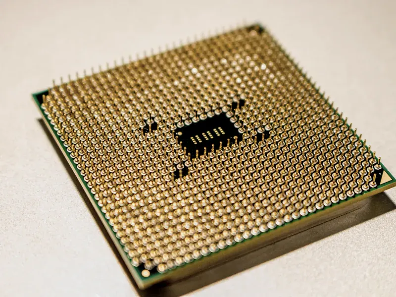
The differences are not incremental—they are categorical. A logistics process designed for packaged ICs will destroy bare die inventory.
1. Electrostatic Discharge: The Invisible Destroyer
A packaged IC routes ESD through protection diodes to the leadframe, safely diverting the discharge away from active circuitry. A bare die has bond pads connected directly to transistor gates. The gate oxide layer in a modern 3nm transistor is approximately 0.5 nm thick—about two atoms of silicon dioxide. A Human Body Model (HBM) discharge of 50V is sufficient to rupture this layer.
The practical implication: every surface that contacts bare die—carrier trays, vacuum wands, inspection fixtures, packaging materials—must be grounded or static-dissipative. The EOS/ESD Association’s 2026 Technology Roadmap identifies Charged Device Model (CDM) events as the fastest-growing risk category as die-level interconnects shrink and gate oxides thin further.
2. Mechanical Fragility: Silicon Is Brittle
Silicon has a fracture toughness of approximately 0.7–1.0 MPa·√m—comparable to window glass. A bare die measuring 5 × 5 mm and thinned to 100 μm (common for stacked memory applications) will fracture under stress levels that a packaged IC would not even register.
Die cracking manifests in two failure modes:
- Catastrophic: Visible edge chipping or full fracture, detectable by visual inspection
- Latent: Micro-cracks that pass visual inspection but propagate under thermal cycling, causing field failures months later
The second category is the procurement nightmare—parts that pass incoming inspection but fail in the field.
3. Oxidation: The Clock Is Ticking
Aluminum bond pads begin oxidizing within hours of exposure to ambient air. Copper bond pads—increasingly common in advanced nodes—oxidize even faster. Once a bond pad surface oxidizes beyond approximately 5 nm of oxide thickness, wire bonding becomes unreliable. The bond wire will not adhere properly, creating an intermittent connection that may pass initial electrical test but fail under thermal or mechanical stress.
The countermeasure: bare die must be sealed in moisture-barrier bags (MBBs) with desiccant and humidity indicator cards (HICs) immediately after dicing. The shelf life for an opened MBB, even in a nitrogen-purged dry box, is measured in days, not weeks.
What Are the Right Carrier Media for Bare Die?
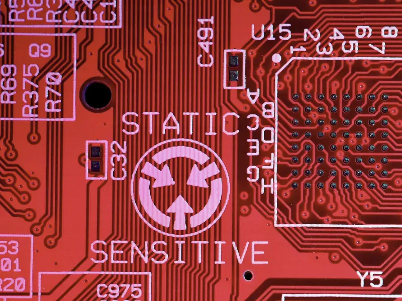
Selecting the appropriate die carrier is the most consequential logistics decision in bare die procurement. The wrong choice at the wrong volume creates either unnecessary cost or unacceptable risk.
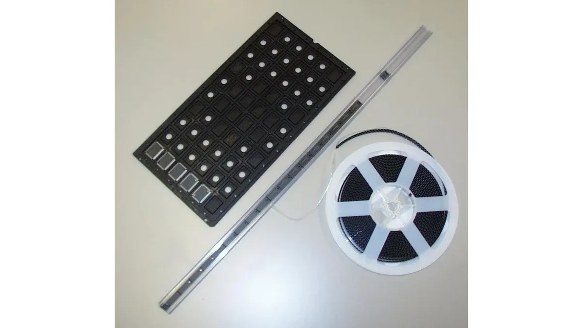
| Carrier Type | Best For | Die Size Range | Volume Range | ESD Protection | Cost Per Die Position |
|---|---|---|---|---|---|
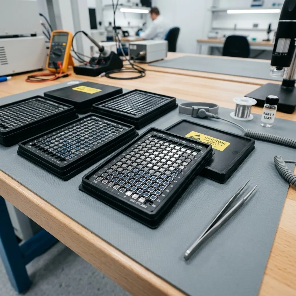
| Waffle Pack | Low-volume, prototyping, sample shipments | 1–25 mm | 1–500 units | Conductive carbon-filled polymer | $0.05–0.15 |
| Gel-Pak | Medium-volume, fragile die, bumped die | 0.5–15 mm | 100–5,000 units | Static-dissipative gel + conductive box | $0.10–0.50 |
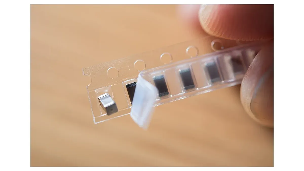
| Tape-and-Reel | High-volume, automated placement | 1–10 mm | 1,000–100,000+ units | Conductive pocket tape | $0.01–0.05 |
| JEDEC Matrix Tray | Standardized handling across multiple lines | 3–40 mm | 50–2,000 units | Static-dissipative or conductive | $0.03–0.10 |
| Wafer Frame (film frame) | Full-wafer transport between fab and packaging | Whole wafer | 100–50,000+ die per wafer | Conductive film on grounded metal frame | $5–20 per frame |
Gel-Pak is the preferred carrier for fragile, bumped, or high-value die in medium volumes. The gel membrane holds each die in place without mechanical clamping, eliminating edge chipping risk during transit. However, Gel-Paks require careful handling during die extraction—an unskilled operator using tweezers can damage the gel surface, compromising protection for the remaining die.
Tape-and-Reel is the only practical option for high-volume automated placement, but it applies mechanical stress to the die during the tape sealing and peeling processes. Die thinner than 100 μm are at elevated risk of fracture during tape handling.
How Should Procurement Teams Qualify Bare Die Logistics Providers?
The certificate on the wall is not enough. Here are the four criteria to audit:
1. ESD Control Program Audited to ANSI/ESD S20.20
Request the full audit report, not just the certificate. Verify that the provider’s ESD protected area (EPA) includes:
- Grounded work surfaces with continuous monitoring
- Personnel grounding via wrist straps and footwear tested at shift start
- Ionizers over workstations handling exposed die
- Regular audit of packaging materials to ANSI/ESD S541
The EOS/ESD Association’s 2026 Technology Roadmap recommends moving beyond voltage control to eliminating conductor-to-conductor contact—a more stringent standard that fewer providers meet.
2. ISO Cleanroom Capability
For bare die inspection or repackaging: ISO Class 5 (Class 100) for wafer-level handling, ISO Class 7 (Class 10,000) minimum for die-level operations in carrier media. A single 0.5 μm dust particle landing on an active bond pad can prevent wire bonding.
3. Chain of Custody with Environmental Monitoring
Request temperature, humidity, and shock data for every handoff in the logistics chain. Providers serving the semiconductor industry should offer real-time environmental monitoring with data loggers that record excursions. An unlogged 4-hour truck transfer in Phoenix in July—where the trailer interior can reach 60°C—can destroy a shipment of bare die that the paperwork says was “temperature controlled.”
4. Insurance That Explicitly Covers Die-Level Loss
Standard cargo insurance often excludes ESD damage, classifying it as “inherent vice” (damage arising from the nature of the goods themselves). Ensure the logistics provider’s insurance policy explicitly covers:
- ESD damage to bare semiconductor die
- Latent damage (failures detected after delivery)
- Full replacement value, not depreciated value
The Demurability Factor: Why OSAT Relationships Matter
As heterogeneous integration grows, the procurement boundary is shifting. Many companies that previously bought packaged ICs are now buying bare die and contracting with OSATs (Outsourced Semiconductor Assembly and Test providers) for packaging.
This creates a procurement coordination challenge: the die supplier, the logistics provider, and the OSAT must operate on compatible carrier formats, environmental controls, and quality documentation standards. A die shipped in a Gel-Pak that arrives at an OSAT expecting tape-and-reel creates a costly rework step and a potential damage exposure.
Best practice: standardize on a single carrier format across your bare die supply chain, and include carrier format specifications in both your die purchase agreements and your OSAT statements of work. When sourcing bare die from major manufacturers like Infineon, STMicroelectronics, or NXP, confirm their standard carrier format before placing orders—carrier mismatch is a leading cause of receiving-side delays.
Shipping bare die or managing a chiplet-based supply chain? SupplyICs provides logistics coordination, carrier format standardization, and qualified bare die sourcing with full environmental monitoring. Contact our logistics team or submit an RFQ for bare die procurement support.
Frequently Asked Questions (FAQ)
How sensitive are bare die to electrostatic discharge compared to packaged ICs?
Bare die are significantly more ESD-sensitive than packaged ICs. A packaged IC has internal ESD protection diodes bonded to the leadframe, providing a discharge path that diverts static away from the active circuitry. A bare die has no such protection—its bond pads are directly exposed to the silicon, and a discharge as low as 50V (Human Body Model) can destroy a gate oxide layer that is only a few atoms thick. Industry estimates from the EOS/ESD Association suggest that over 30% of semiconductor failures during manufacturing and handling are ESD-related, and for bare die, the failure rate in unmanaged environments can exceed 50%. The cost of a single ESD-induced failure ranges from a few cents for a simple diode to thousands of dollars for a complex processor die.
What are the essential handling requirements for bare die logistics?
Bare die logistics require five layers of protection: (1) Carrier media—waffle packs for small die counts, Gel-Paks for medium volumes, tape-and-reel for high-volume automated placement; (2) ESD shielding—conductive or static-dissipative containers that create a Faraday cage around the die; (3) Desiccant and humidity indicator cards inside sealed moisture-barrier bags (MBBs) to prevent oxidation of aluminum or copper bond pads; (4) Temperature-controlled transport (15–25°C) to prevent thermal cycling stress; and (5) Shock/vibration isolation through foam-lined outer packaging. Every person handling bare die must wear a grounded wrist strap, ESD-safe footwear, and ESD-safe garments in an EPA (ESD Protected Area) with grounded work surfaces and ionizers.
How do I qualify a logistics provider for bare die shipping?
Qualify bare die logistics providers against four criteria: (1) ESD control program audited to ANSI/ESD S20.20—request the audit report, not just the certificate; (2) Cleanroom capability (ISO Class 5–7 depending on die sensitivity) for any repackaging or inspection steps; (3) Chain of custody documentation showing temperature, humidity, and shock data for every handoff; and (4) Insurance coverage that explicitly includes ESD damage and die-level loss. Conduct an on-site audit before qualifying, and requalify annually. Preferred providers maintain SEMI E78, E129, and E163 compliance for electrostatic monitoring in wafer-level environments.