
Table of Contents
Infineon’s new 200 mm silicon carbide (SiC) wafer agreement is a meaningful upstream supply development. A buyer of finished MOSFETs or power modules has a narrower question: which approved devices, if any, gain a different supply path, and when can those devices be delivered?
As of October 16, 2026, the latest agreement from Infineon and earlier manufacturing announcements provide evidence of the transition. They support a closer look at qualification and sourcing plans, rather than an automatic forecast of cheaper devices or shorter lead times.
What changed in the 200 mm SiC supply chain?
Infineon announced a new multi-year agreement with Wolfspeed for 200 mm SiC wafers on October 15, 2026, extending their supply relationship into the larger substrate format. That is an upstream procurement milestone, not a finished-device delivery schedule.
The Infineon announcement connects the agreement to its conversion from 150 mm to 200 mm manufacturing and broader substrate sourcing. It does not disclose allocation for a particular MOSFET ordering code or guarantee a customer’s qualification timeline.
A separate earlier milestone was Wolfspeed’s September 10, 2025 commercial materials launch, covering 200 mm bare wafers and epitaxy offered for qualification. Materials availability and device availability remain different stages.
Another manufacturer’s roadmap illustrates the timing distinction. ST’s May 31, 2024 Catania announcement targeted a production start in 2026 and a full ramp by 2033. Those are the targets stated in that announcement; it does not establish that the planned 2026 milestone has occurred.
Does a larger SiC wafer guarantee cheaper MOSFETs?
No. A larger wafer provides more gross surface area, but finished-device economics also depend on usable area, defect distribution, die size, process yield, equipment costs and downstream assembly and test.
For ideal circles, increasing diameter from 150 mm to 200 mm changes gross area by:
(200 ÷ 150)² = 1.7778, or approximately 77.8% more area.
That calculation excludes edge losses, test structures and yield. It is not a prediction of 77.8% more good dies or a proportional price reduction. An actual die layout has discrete packing constraints, and a process ramp may change costs and yields over time.
For quote comparisons, keep the finished ordering code, quantity, delivery window and qualification scope constant. A lower price on a different die or package is a separate engineering comparison. The wafer-area calculation alone supplies no defensible discount target.
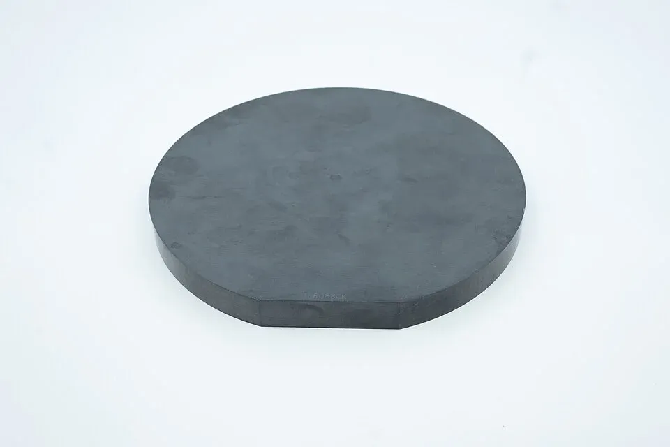
From substrate to qualified device
The flow must connect substrate quality, device fabrication, assembly and test, and customer approval. Progress at one stage does not remove the evidence needed at the next.
| Stage | Question for the sourcing review | What the stage alone cannot establish |
|---|---|---|
| Substrate and epitaxy | Are the required material specifications qualified? | Finished MOSFET characteristics or package availability |
| Device process | Is the intended device flow qualified at the applicable site? | Completed package and application approval |
| Assembly and test | Are package, interconnect and screening requirements met? | Compatibility with every gate driver or thermal design |
| Customer application | Has the exact device passed the product’s approval process? | Capacity or delivery rights beyond the accepted order |
Start with the manufacturer’s product change notification when a transition affects the purchased part. Match its ordering codes, affected lots or revisions and implementation date to the approved BOM. A public wafer agreement by itself is not a reason to requalify an unchanged device.
If the notice includes a die, process or package change, engineering should define the affected qualification scope. For a power-switching design, that may include conduction losses, switching behavior, gate-drive requirements and thermal performance under the existing operating conditions. Use the changed device’s data and notification; wafer diameter does not identify which of those characteristics changed.
The SiC versus GaN sourcing comparison addresses a different decision: choosing a device technology for the application. Once SiC is selected, wafer diameter is still only one factor within the manufacturer’s production flow.
How should a buyer use this transition in a 2027 sourcing plan?
Keep the existing approved device in the production plan while evaluating any proposed transition as a separate change. Ask the supplier to connect the 200 mm roadmap to orderable products, applicable change notices and qualification schedules.
A useful supplier update answers three questions: which ordering codes are affected, when representative samples and qualification results will be available, and which accepted delivery schedule benefits after approval. If the update covers only substrate capacity, it belongs in the market watch rather than confirmed build coverage.
Agree the handover before changing the purchase line. That includes any customer approval, lot identification, treatment of existing stock and the point at which the new flow is permitted. If qualification slips, confirm how the approved flow will cover the intervening builds instead of assuming both flows remain available indefinitely.
The transition can improve future sourcing flexibility, but the practical trigger is a qualified device and a supported shipment schedule. Continue to compare delivered cost and execution as the ramp develops; a delayed factory milestone or weaker customer demand can change the timing of the expected benefit.
Frequently Asked Questions (FAQ)
Does a 200 mm substrate agreement identify the wafer source of every finished device?
No. The announcement describes an upstream supply relationship. Exact device sourcing and change information must come from the manufacturer’s applicable product and qualification records.
Should buyers reject a qualified 150 mm-based SiC device because 200 mm production is expanding?
No. Wafer diameter alone does not determine application suitability. Continue to evaluate the finished device’s electrical, thermal, reliability and supply requirements.
Can a planned factory start date be treated as proof of current output?
No. A plan establishes an intended milestone. Confirm commissioning, production and product qualification separately before using new capacity as evidence of delivery coverage.