
Table of Contents
- CHIPS Act Fab Scorecard: Mid-2026 Project-by-Project Status
- Category 1: In Volume Production
- Category 2: Under Construction — Production Start H2 2026 to H2 2027
- Category 3: Under Construction — Production Start 2028-2030
- Three Developments That Changed the Scorecard This Quarter
- 1. Intel 18A: Real Silicon, Real Customers, Unanswered Questions
- 2. Ohio Module 2: The $3 Billion Delay
- 3. Samsung Taylor: The 2nm-Only Pivot
- Is U.S. Reshored Manufacturing Actually Reshoring Jobs and Supply Chain?
- Jobs: The Act Is Delivering
- Supply Chain Independence: It’s a 2030 Story
- What Does the Scorecard Mean for Procurement in 2026-2029?
- 2026-2027: Limited Procurement Impact
- 2028-2029: The Capacity Inflection Begins
- 2030 and Beyond: A Genuinely Diversified Supply Base
In January 2026, Intel’s Fab 52 in Chandler, Arizona began shipping 18A revenue wafers to paying foundry customers. This is the most advanced logic process node (1.8nm-class, RibbonFET gate-all-around transistors with PowerVia backside power delivery) ever manufactured at volume on American soil.
Three months later, TSMC confirmed that its Arizona Fab 21 Phase 1 was running 24,000 wpm of N4 (4nm) capacity—with Apple, AMD, and NVIDIA confirmed as initial customers. Samsung Taylor Fab 1 had reached 15,000 wpm of 3nm GAA production. After three decades of advanced logic manufacturing gravitating almost entirely to Taiwan and Korea, leading-edge transistors are being fabricated in the United States again.
The significance is real. The timeline for procurement impact is longer than the headlines suggest.
Related Reading: This article is a fab-level scorecard update. For the broader policy narrative and how CHIPS Act reshoring affects global supply chains, see CHIPS Act and Semiconductor Reshoring: Mid-2026 Progress Report. For lead time data by foundry, see CHIPS Act Reshoring: Fab Capacity and Lead Times Analysis.
📌 Direct Answer: The CHIPS Act has funded $38.7 billion of its $39 billion manufacturing incentives pool across 23 recipients as of May 2026, with $11 billion physically disbursed against verified construction and equipment milestones. Three fabs are in production, 14 more are under construction, and the total U.S. advanced logic manufacturing share has risen from 12% (2020) to approximately 22% (2026) per SIA estimates. But these numbers need context: the three operating fabs represent only 8% of global advanced-node capacity, their output is overwhelmingly allocated to the largest customers (Apple, NVIDIA, AMD, Amazon, Microsoft), and U.S.-manufactured wafers carry a 20-30% structural cost premium over Taiwan equivalents. For procurement teams at mid-size OEMs, reshored capacity is real but not meaningfully accessible before 2028-2029 when the fabs currently under construction reach mature yields.
CHIPS Act Fab Scorecard: Mid-2026 Project-by-Project Status
Category 1: In Volume Production
| Fab | Company | Location | Process Node | Capacity (wpm) | CHIPS Award | Production Start | Key Customers | Procurement Significance |
|---|---|---|---|---|---|---|---|---|
| Fab 52 | Intel | Chandler, AZ | 18A (RibbonFET) | 30,000 | $8.5B | Q1 2026 | Intel internal, Amazon (Trainium 3), Microsoft | First 18A volume production; Intel Foundry external customer ramp still early |
| Fab 21 P1 | TSMC | Phoenix, AZ | N4 (4nm FinFET) | 24,000 | $6.6B | Q1 2026 | Apple, AMD, NVIDIA | Most advanced non-Intel US logic; ~8-10% of TSMC N4 capacity |
| Fab 1 | Samsung | Taylor, TX | 3nm GAA (SF3) | 15,000 | $6.4B | Late 2025 | Samsung LSI (internal), mobile SoC customers | Only GAA production outside Korea; yield rates estimated 60-70% |
Total In-Production Capacity: 69,000 wpm (300mm equivalent)
Category 2: Under Construction — Production Start H2 2026 to H2 2027
| Project | Company | Process | Planned Capacity | CHIPS Award | Target Production | Status |
|---|---|---|---|---|---|---|
| RFAB3 (Sherman) | Texas Instruments | 28nm-130nm analog/embedded | 50,000 wpm | $1.6B (combined) | H2 2026 | Near complete; equipment move-in underway |
| LFAB2 (Lehi) | Texas Instruments | 28nm-130nm analog/embedded | 40,000 wpm | $1.6B (combined) | Q1 2027 | Equipment installation; 300mm conversion from former Micron IM Flash fab |
| Fab 21 P2 | TSMC | Phoenix, AZ | N3 (3nm FinFET) | $6.6B (combined) | H2 2027 | Shell complete; equipment installation Q3 2026 |
| Fab 62 | Intel | Chandler, AZ | 18A → 14A | $8.5B (combined) | H2 2027 | Under construction; shell complete |
| Module 1 (Ohio) | Intel | New Albany, OH | 18A → 14A | $8.5B (combined) | H2 2027 | Shell nearing completion; equipment installation H1 2027 |
| Boise Fab 1 | Micron | Boise, ID | DRAM 1β/1γ | $6.1B | 2027 | Under construction |
Category 3: Under Construction — Production Start 2028-2030
| Project | Company | Process | Planned Capacity | CHIPS Award | Target Production | Status |
|---|---|---|---|---|---|---|
| Fab 21 P3 | TSMC | Phoenix, AZ | N2 or A14 | 24,000 wpm | $6.6B (combined) | 2029-2030 |
| Fab 2 | Samsung | Taylor, TX | 2nm GAA (SF2) | $6.4B (combined) | 2028 | Under construction; pivot from 4nm to 2nm-only |
| Module 2 (Ohio) | Intel | New Albany, OH | 14A | 30,000 wpm | $8.5B (combined) | 2030 (delayed from 2027-2028) |
| Clay Fab 1 | Micron | Clay, NY | DRAM 1γ/1δ | $6.1B (combined) | 2028-2029 | Site preparation; H2 2026 construction start |
| West Lafayette | SK Hynix | West Lafayette, IN | HBM Advanced Packaging | N/A (packaging) | $1.2B | 2028 |
| Malta Expansion | GlobalFoundries | Malta, NY | 28nm-130nm (incl. GaN) | $800M | 2027-2028 | Under construction |
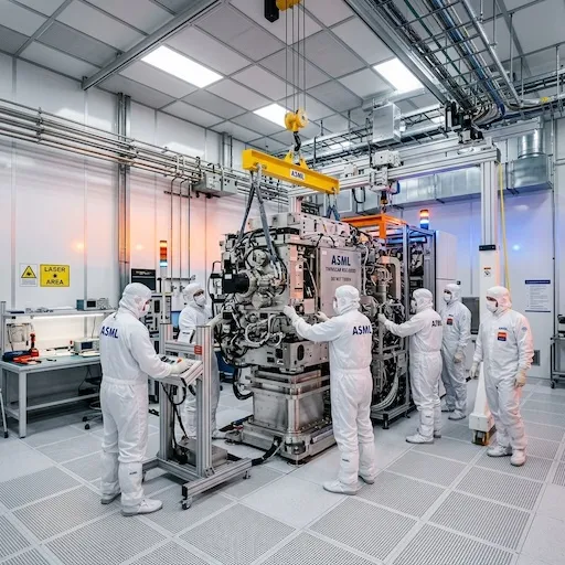 Fig 1: Semiconductor fab cleanroom under construction at a CHIPS Act-funded facility. Equipment installation represents the critical-path milestone between “shell complete” and “volume production.”
Three Developments That Changed the Scorecard This Quarter
1. Intel 18A: Real Silicon, Real Customers, Unanswered Questions
Intel 18A reaching HVM (High-Volume Manufacturing) at Fab 52 in Q1 2026 is the single most significant milestone in the CHIPS Act scorecard. The 18A process node—Intel’s first to combine RibbonFET gate-all-around transistors with PowerVia backside power delivery—is a genuinely competitive leading-edge technology. Intel is manufacturing its own Panther Lake (client) and Clearwater Forest (server) products on 18A, plus foundry wafers for Amazon (Trainium 3 AI accelerator) and Microsoft.
The unanswered question is yield. Intel has not publicly disclosed 18A defect density data, and industry sources offer conflicting accounts ranging from “competitive with TSMC N3 at equivalent maturity” to “still below 0.1 defects/cm² and struggling with SRAM yield.” For procurement teams evaluating Intel Foundry Services as a second source to TSMC, yield directly determines effective wafer cost: if 18A yields trail TSMC N3 by 15-20 percentage points, the per-good-die cost at Intel may exceed TSMC despite potentially lower quoted wafer pricing.
Intel Foundry’s external customer ramp also remains nascent. Amazon and Microsoft are strategic anchor tenants who received preferential pricing and capacity guarantees that may not be available to smaller fabless customers. For a mid-size chip company shipping 5,000-10,000 wpy (wafers per year), Intel Foundry Services in mid-2026 is more of a future option than a current procurement reality.
2. Ohio Module 2: The $3 Billion Delay
Intel’s decision to delay Ohio Module 2 to 2030—announced quietly in its Q1 2026 earnings call—was the most significant negative revision in the CHIPS Act fab scorecard. The original plan called for two Ohio modules (each 30,000 wpm) ramping in 2027-2028, creating a combined 60,000 wpm of leading-edge capacity. Module 1 remains on track; Module 2 is effectively a 2030 project.
The delay exposes the financial tension at the heart of the CHIPS Act model. Building a greenfield fab in Ohio—where no semiconductor manufacturing ecosystem exists—costs approximately $3 billion more than an equivalent expansion at Intel’s existing Arizona campus, where shared infrastructure (ultrapure water, bulk gas pipelines, chemical supply chains, equipment service networks) already exists. With Intel Foundry Services still developing its external customer base and Intel’s own product roadmap requiring less 18A/14A capacity than originally forecast, the incremental Ohio module didn’t clear the return-on-investment hurdle.
For procurement, the Ohio delay means less leading-edge U.S. capacity in the 2027-2029 window than previously expected. Combined with TSMC’s measured pace of Arizona expansion (Phase 3 targeting 2029-2030), the U.S. will remain a minority source of advanced logic supply through the end of the decade.
3. Samsung Taylor: The 2nm-Only Pivot
Samsung’s decision to abandon the originally-planned 4nm capacity at Taylor and produce exclusively on 2nm GAA (SF2) starting in late 2026 is a high-risk, high-reward strategic bet. The rationale: TSMC’s 4nm (N4) is the industry’s most proven, highest-volume advanced node, and Samsung’s 4nm-class process (SF4E/SF4) has struggled to win meaningful foundry market share. Competing with TSMC N4 on volume and cost from a new U.S. fab was a losing proposition.
Instead, Samsung is betting that SF2—its second-generation GAA node with backside power delivery (BSPDN)—can leapfrog TSMC’s N2 (which uses FinFET, not GAA) on performance per watt for HPC and AI accelerator applications. If the bet pays off, Samsung Taylor becomes the only source of GAA+BSPDN logic manufacturing in the United States, with a potentially compelling value proposition for fabless AI chip companies seeking a differentiated process technology. If it doesn’t—if SF2 yields follow the same challenging trajectory as Samsung’s earlier GAA nodes—Taylor becomes a very expensive underutilized asset.
For procurement, the practical implication is that Samsung Taylor will not produce wafers in commercially meaningful volumes before late 2026 at the earliest, and the 2nm-only focus means no overlap with the 3nm-4nm capacity that currently represents the bulk of advanced logic demand.
Is U.S. Reshored Manufacturing Actually Reshoring Jobs and Supply Chain?
The CHIPS Act’s economic rationale combined national security (reduce dependence on Taiwan for advanced logic) with domestic manufacturing employment. The jobs side of the equation is materializing; the supply chain independence side is more complicated.
Jobs: The Act Is Delivering
TSMC Arizona directly employs approximately 2,200 workers across Phase 1 (operations) and Phase 2 (construction). Intel’s Arizona and Oregon expansions have added roughly 5,000 direct manufacturing jobs. Samsung Taylor employs approximately 1,200. Texas Instruments’ Sherman and Lehi expansions will add an estimated 3,000 direct jobs. The Construction industry estimates that each direct semiconductor manufacturing job supports 5-7 indirect jobs in construction, equipment service, logistics, and local services.
At full buildout (2028-2030), the CHIPS Act-funded projects are expected to support approximately 50,000 direct semiconductor manufacturing jobs and 250,000-350,000 indirect jobs—meaningful but a fraction of Taiwan’s semiconductor workforce (approximately 280,000 direct jobs in the Hsinchu, Tainan, and Kaohsiung science parks alone).
Supply Chain Independence: It’s a 2030 Story
The fabs are being built. The supporting ecosystem—the network of equipment suppliers, bulk gas plants, chemical manufacturers, substrate vendors, and silicon wafer producers that make a fab cluster efficient—is much slower to materialize. TSMC Arizona still sources the majority of its ultrapure water systems, bulk gas purification, and specialty chemicals from the same Asian suppliers that serve its Taiwan fabs, simply because those suppliers do not have U.S. manufacturing operations at scale.
The CHIPS Act recognized this: the NSTC (National Semiconductor Technology Center), NAPMP (National Advanced Packaging Manufacturing Program), and workforce development programs collectively represent $10B+ in R&D and ecosystem investment. But ecosystem development is measured in decades, while fab construction is measured in years. The U.S. will have advanced manufacturing facilities before it has an advanced manufacturing ecosystem.
What Does the Scorecard Mean for Procurement in 2026-2029?
2026-2027: Limited Procurement Impact
The three operating fabs (69,000 wpm combined) overwhelmingly serve the largest semiconductor consumers: Apple, NVIDIA, AMD, Amazon, Microsoft, and Samsung LSI. For procurement teams at mid-size OEMs, EMS providers, or fabless chip companies, the U.S. fab capacity that is genuinely accessible in 2026 is effectively zero. The wafer output is fully committed to the anchor tenants who signed capacity agreements as a condition of CHIPS Act funding.
Practical implication: Do not plan your 2026-2027 procurement strategy around U.S.-based advanced logic supply. It will not be available to you.
2028-2029: The Capacity Inflection Begins
When TSMC Fab 21 Phase 2 (N3, 24,000 wpm) and Intel Fab 62 and Ohio Module 1 (18A/14A, 60,000 wpm combined) reach volume production in 2027-2028, the U.S. advanced logic capacity base will roughly double to approximately 150,000 wpm. At that scale, some capacity should become accessible to customers beyond the top five.
This is the window when procurement teams should begin actively qualifying U.S.-based fab sources. If your chip supplier currently manufactures exclusively at TSMC Taiwan, ask about Arizona wafer supply options. If your supplier uses Samsung Korea, investigate Taylor availability. The availability will be incremental—these fabs will not be running at 50% utilization looking for customers—but having U.S.-based wafer supply as a qualified option expands your supply chain resilience.
2030 and Beyond: A Genuinely Diversified Supply Base
At full buildout—all three TSMC Arizona phases (72,000 wpm), multiple Intel Arizona/Ohio modules (120,000+ wpm combined), Samsung Taylor Phase 1 and 2 (35,000+ wpm), plus the memory and analog fabs—the U.S. will have roughly tripled its 2025 advanced logic manufacturing capacity. At that scale, U.S.-based wafer supply becomes a meaningful percentage of global capacity rather than a niche geopolitical hedge, and market forces (rather than allocation politics) begin determining which customers get access.
The timeline is credible because the facilities are physically under construction, not proposed. But it is a 2030 story, not a 2026 one.
SupplyICs tracks CHIPS Act fab construction progress, wafer capacity additions, and lead time data across all major foundries. Our procurement team can help you evaluate when and how U.S.-based wafer supply becomes a viable sourcing option for your specific component requirements. Contact our market intelligence team for a BOM-level reshoring impact assessment.
Frequently Asked Questions (FAQ)
Which CHIPS Act-funded fabs are actually producing wafers in mid-2026?
Three major CHIPS Act-funded logic fabs are in volume production as of mid-2026: Intel Fab 52 Arizona (18A, 30,000 wpm), TSMC Arizona Fab 21 Phase 1 (N4, 24,000 wpm), and Samsung Taylor Fab 1 (3nm GAA/SF3, 15,000 wpm). Combined, these represent approximately 69,000 wpm of leading-edge U.S.-based logic capacity—roughly 8% of global advanced-node capacity. An additional 14 CHIPS Act projects are under construction with staggered production starts from late 2026 through 2030. Micron's Boise DRAM fab and Texas Instruments' Sherman RFAB3 are expected to begin production in H2 2026.
Why was Intel's Ohio fab delayed to 2030?
Intel's Ohio Module 2 (originally targeting 2027-2028 production) was delayed to 2030 due to three converging factors: (1) a slower-than-expected ramp of Intel Foundry Services external customer volume, reducing the near-term demand for additional 18A/14A capacity beyond what Arizona provides; (2) construction cost escalation—Ohio's greenfield site required approximately $3 billion more in site preparation and utility infrastructure than originally budgeted; and (3) Intel's strategic decision to prioritize its Arizona and Oregon fab expansions where existing infrastructure reduces per-wafer cost. The delay does not affect Module 1 (Ohio), which remains on track for H2 2027.
Are reshored US wafers actually more expensive than Taiwan-manufactured wafers?
Yes. U.S.-manufactured wafers cost approximately 20-30% more than equivalent Taiwan-manufactured wafers on the same process node. This cost gap is structural rather than transitional: U.S. fab construction costs 2-4x more per square foot of cleanroom, U.S. technician and engineer salaries are 40-50% higher, and the U.S. lacks Taiwan's clustered supplier ecosystem (bulk gases, chemicals, equipment service) that reduces operating costs. The CHIPS Act Investment Tax Credit (25%) partially offsets capital costs but does not address the ongoing opex disadvantage. Procurement teams should not expect reshored manufacturing to deliver cost savings—its value is supply chain diversification and geopolitical risk reduction.