Table of Contents
- Which input and output formats must a clock buffer support?
- How can clock-buffer additive-jitter specifications be compared fairly?
- How does clock-buffer skew reduce timing margin?
- Design the load and termination with the buffer
- Measure power-noise sensitivity in the real board
- What happens to clock outputs during disable, startup, or clock loss?
A clock buffer distributes an edge that every downstream receiver treats as a timing reference. Frequency and channel count are only the starting fields. Signal format, input sensitivity, phase noise, skew, output loading, termination, supply noise, and power-state behavior determine the usable timing margin.
Create a system jitter and skew budget before comparing devices. The buffer should consume a defined share of that budget under the same measurement assumptions used for the source and receiver.
Which input and output formats must a clock buffer support?
The clock buffer must accept the source’s signal format, amplitude, common-mode range, slew rate, and coupling while driving the format required by each receiver. Identify whether the interface is LVCMOS, LVDS, LVPECL, HCSL, CML, sine, or another specified standard before comparing channel count and frequency.
For a differential input, determine whether unused complementary input handling and AC-coupling bias are built in. For LVCMOS, confirm supply voltage, threshold compatibility, duty-cycle requirements, and input rise/fall limits.
How can clock-buffer additive-jitter specifications be compared fairly?
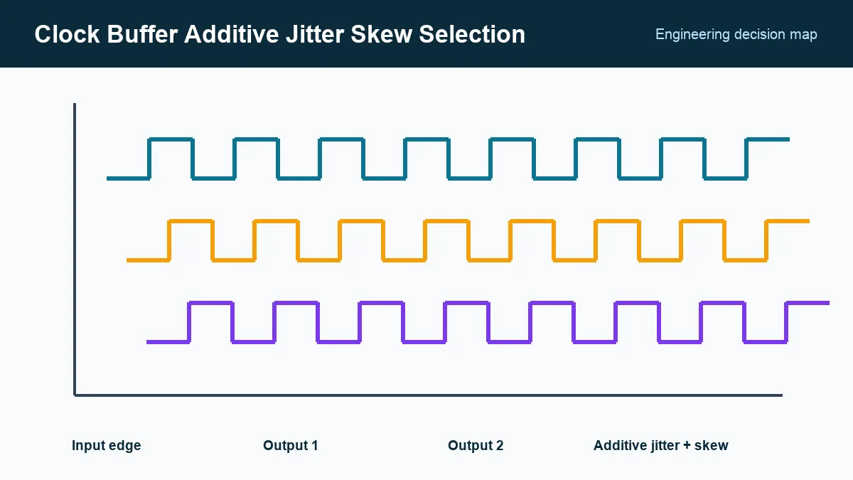
Compare additive-jitter values only under compatible integration bandwidths, carrier frequencies, input slew and noise conditions, output formats, and measurement methods. Additive jitter describes the buffer’s contribution beyond the source; a smaller number measured over a narrower band does not establish a better result in the receiver’s relevant band.
Renesas application note 804, accessed September 24, 2026, discusses measuring additive phase jitter by comparing input and output phase noise. Retain the integration limits with every comparison.
For uncorrelated RMS terms, a first-order budget combines them by root-sum-square. If the source jitter is already near the receiver limit, calculate the remaining allowable buffer and distribution contribution rather than selecting from a generic “low jitter” label.
How does clock-buffer skew reduce timing margin?
Clock-buffer skew shifts the clock arrival time between receiving paths and consumes the corresponding setup or hold margin. Budget channel-to-channel skew for outputs on one buffer and part-to-part variation across separate buffers, then include package, PCB trace, connector, and receiver clock-distribution differences.
Texas Instruments’ clock-buffer portfolio overview, accessed September 24, 2026, separates output technologies and clock-distribution functions. Use the detailed data sheet for skew limits across process, voltage, temperature, and loading; typical room-temperature values do not form a production budget.
Duty-cycle distortion can turn into setup or hold loss in double-data-rate or edge-sensitive systems. Compare high and low pulse-width limits in addition to propagation delay.
Design the load and termination with the buffer
Each signaling standard has a source, line, and receiver model. Confirm output impedance, required bias, termination voltage, DC current, trace impedance, and receiver loading. Do not copy an LVDS or HCSL termination across devices without checking whether the buffer includes internal resistors.
For LVCMOS, a source-series resistor can control the first launched edge when the topology is one source to one receiver. Stubs and multiple loads require transmission-line analysis. Faster edges can increase ringing and crosstalk even when the clock frequency is unchanged.
Measure power-noise sensitivity in the real board
Separate and decouple buffer supply domains as recommended. Power-supply noise can modulate threshold and delay. Measure spurs and jitter with the production regulator, load activity, and adjacent switching circuits operating.
Inject or reproduce the dominant rail ripple when margin is tight. Compare the measured clock spectrum with the regulator switching frequency and its harmonics so a supply-created spur is not misclassified as random buffer jitter.
What happens to clock outputs during disable, startup, or clock loss?
Clock-output behavior depends on the selected buffer: outputs may stop low, stop high, or retain their last state under defined conditions. Check enable transitions, loss of input clock, and missing supplies in the exact data sheet, then test for runt pulses as well as startup delay.
Qualification should measure frequency range, duty cycle, output waveform, channel skew, startup, enable/disable, phase noise or jitter, and power sensitivity across voltage and temperature. Release records should include buffer ordering code, source conditions, formats, termination, output loads, integration bandwidth, jitter allocation, skew allocation, layout constraints, and power-state table. That package lets a replacement be judged within the actual clock tree.
Frequently Asked Questions (FAQ)
Is additive jitter simply added arithmetically to source jitter?
Independent RMS jitter contributions are commonly combined by root-sum-square, but only after using compatible definitions, bandwidths, filters, and units. Deterministic or correlated components need separate treatment.
What is the difference between output skew and part-to-part skew?
Output skew compares channels on one device under defined conditions. Part-to-part skew adds variation across different devices, lots, supplies, temperatures, and often different boards.
Can an LVCMOS clock output drive several receivers directly?
Only if fanout, load capacitance, trace topology, edge rate, voltage, and reflections remain within all receiver and buffer limits. Separate buffered outputs are usually easier to time and terminate.