Table of Contents
- Describe the Sensor Source Before Comparing Amplifiers
- Fit Input Common Mode and Output Swing Together
- Set Gain Without Losing Bandwidth or Headroom
- Refer Every Error Term Back to the Sensor
- Control Input Protection, Filtering, and Settling
- Decide Where Calibration Helps
- Validate Layout, Temperature, and the Exact Grade
An instrumentation amplifier is selected around a sensor and an ADC, not from offset voltage alone. The source impedance and common-mode voltage determine what reaches the inputs; gain and reference voltage determine where the output lands; protection, filtering, noise, and drift determine how much of the sensor signal remains useful.
The decisive check is whether the amplifier stays linear at every combination of differential input, common mode, gain, supply, reference, load, and temperature. A part can accept input voltages inside its published rails and still saturate an internal stage or the output.
Describe the Sensor Source Before Comparing Amplifiers
Record the sensor type, full-scale differential output, zero output, source impedance on each lead, expected common-mode voltage, source imbalance, bandwidth, cable length, excitation method, and fault exposure. A bridge transducer, thermocouple, shunt, and biopotential electrode all present different impedance, bias-current, protection, and noise requirements.
Decide whether the source is floating or ground-referenced and where input bias current can return. A floating source without a bias-current path can drive the inputs to an undefined common-mode level. Large input resistors can create that path, but their leakage, noise, mismatch, and interaction with protection need to enter the error budget.
Instrumentation amplifiers are not a universal replacement for every differential amplifier. A current-sense amplifier is designed around a shunt and often tolerates common mode far beyond its own supply. An isolation amplifier crosses a galvanic barrier. A fully differential amplifier is commonly used to drive a differential ADC and may not offer the same input impedance or gain programming. Keep those tasks separate in the candidate list.
Fit Input Common Mode and Output Swing Together
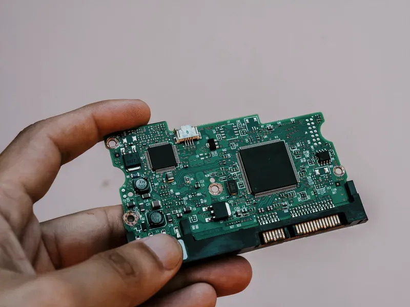
The allowable input common-mode range usually depends on gain and output level. Inside a classic three-amplifier instrumentation architecture, the input amplifiers and output difference stage each require headroom. Raising gain can force internal nodes farther apart even if the external differential input is small.
For every corner, calculate or plot input common mode, differential input, selected gain, reference voltage, and expected output. Include sensor overrange, startup, a disconnected lead, input protection conduction, supply tolerance, and reference-source tolerance. Compare these states with the manufacturer’s input common-mode versus output-voltage guidance, not just a single table row.
Single-supply operation is especially easy to misread. “Rail-to-rail input” and “rail-to-rail output” are conditional phrases, and many instrumentation amplifiers do not provide either across every gain and load. The TI instrumentation amplifier overview explains the architecture and common-mode rejection benefit, but the exact orderable device’s data sheet governs headroom.
Set the REF pin deliberately. It usually shifts the output baseline; it is not an arbitrary high-impedance logic input. Verify its input current, impedance, noise contribution, permitted source resistance, and decoupling. A weak divider can add gain or common-mode error if the reference node moves with load or ADC sampling.
Set Gain Without Losing Bandwidth or Headroom
Choose gain from the minimum and maximum sensor signal, offset, expected fault/overrange, reference level, amplifier output swing, ADC input range, and desired guard band. Do not use the entire nominal ADC span; leave room for sensor tolerance, amplifier error, reference error, supply variation, and transient recovery.
Some instrumentation amplifiers use a single external gain resistor; others provide fixed gains, pins, or a digital interface. For an external resistor, include equation tolerance, resistor tolerance and temperature coefficient, PCB leakage, and any gain-dependent specifications. Keep the resistor close to the device and away from contamination or high-voltage nodes when its value is large.
Bandwidth generally decreases as gain rises, and settling can be more important than small-signal bandwidth in multiplexed or pulsed measurements. Check gain-bandwidth, large-signal slew, overload recovery, and settling to the required resolution. A 10 kHz bandwidth claim does not show that the output settles to 16-bit accuracy after a sensor switch or protection event.
The Analog Devices instrumentation-amplifier catalog and Microchip instrumentation-amplifier portfolio expose different filters and specification columns. Normalize them around the sensor and converter rather than comparing whichever typical values appear in both selectors.
Refer Every Error Term Back to the Sensor

Convert errors to one common point before adding them. Input-referred voltage is usually convenient: amplifier offset is already input-referred, output noise can be divided by gain, and ADC/code error can be divided by the complete signal-chain gain. Then convert the total to the sensor’s physical unit if required.
| Error term | Usually dominates when | What to verify |
|---|---|---|
| Input offset and drift | Low-level DC measurement | Maximum over temperature and any warm-up condition |
| Input bias current | High or imbalanced source impedance | Maximum current, return path, source-resistance mismatch |
| Gain error and drift | Near full scale | Selected gain, external resistor, temperature |
| CMRR | High or changing common mode | Frequency, gain, source balance and resistor matching |
| Voltage/current noise | Low signal or wide bandwidth | Spectral density, 0.1–10 Hz noise and integrated bandwidth |
| Output/ADC error | Range endpoints and sampling | Output load, reference, acquisition kickback and headroom |
Do not add all maxima arithmetically unless the requirement truly calls for worst-case alignment; do not combine them as root-sum-square without identifying uncorrelated contributors. Report both the deterministic limit and an appropriate statistical model when the product’s quality process permits one.
Common-mode rejection ratio (CMRR) can be specified at DC and degrade with frequency. External input filters and source resistance can convert common-mode interference into a differential error if the two sides do not match. The error may then be dominated by passive mismatch rather than the amplifier’s headline CMRR.
Control Input Protection, Filtering, and Settling
Start from credible faults: electrostatic discharge, cable transients, sensor excitation short, overvoltage, a powered sensor connected to an unpowered amplifier, or an input driven while a supply is missing. Absolute-maximum input current and voltage are survival limits, not measurement conditions.
Series resistors, clamps, transient suppressors, and RC filters add leakage, thermal noise, bias-current drop, capacitance, and mismatch. Check the original equipment manufacturer’s input-protection recommendations and simulate or calculate fault current across component tolerance and temperature. If external diodes are used, their leakage at high temperature can exceed the amplifier’s own input bias.
For a differential RC filter, match both paths and include capacitor tolerance. A differential capacitor can control differential noise while equal common-mode capacitors may improve radio-frequency filtering, but mismatch can reduce high-frequency CMRR. Confirm stability and settling after the filter, especially when the output drives a sampling ADC.
Decide Where Calibration Helps
A zero calibration can remove the combined initial offset of the sensor, amplifier, and ADC at one temperature and common-mode condition. A span calibration can remove initial gain error using a traceable stimulus. Store the calibration state, equipment uncertainty, temperature, gain configuration, reference state, and coefficient version.
Calibration does not fix clipping or insufficient common-mode headroom. It also cannot fully remove temperature drift unless the product characterizes and models temperature, and it does not remove random noise. If the signal path changes gain, sensor excitation, multiplexed channel, or reference source, determine whether the same coefficients remain valid.
Chopper or auto-zero amplifiers can reduce low-frequency offset and drift while adding switching artifacts, ripple, input-current transients, or aliasing concerns. Evaluate their spectral behavior within the real filter and sampling plan rather than equating “zero drift” with zero error.
Validate Layout, Temperature, and the Exact Grade
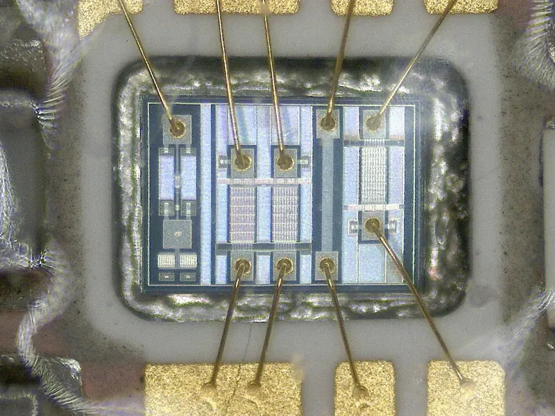
Route sensor inputs as a balanced pair, keep them away from switch nodes and digital edges, and provide a controlled return for shields and bias currents. Protect high-impedance nodes from contamination and flux residue. Place the gain resistor and decoupling components according to the data sheet, and route the REF node as a precision analog signal.
Test zero, midscale, and full-scale differential inputs across common-mode range, supply range, gain settings, output load, and temperature. Add common-mode steps, overload and recovery, cable interference, power sequencing, and the final ADC acquisition. Measure the physical sensor path when possible; a signal generator with near-zero source impedance can conceal bias and leakage errors.
Control the exact device suffix, package, temperature grade, gain option, and qualification. For an alternate, repeat the headroom and error budget using its guaranteed limits, then validate its protection and settling on the same board. That record turns “precision amplifier” into an auditable signal-chain decision rather than a label attached to a low typical offset.
Frequently Asked Questions (FAQ)
When should an instrumentation amplifier be used instead of an op amp?
Use an instrumentation amplifier when a small differential sensor signal must be measured with high input impedance while a larger common-mode voltage is present. Its matched internal network and specified gain and common-mode rejection can be more predictable than a discrete op-amp difference stage, but input and output ranges still require verification.
How does input common-mode voltage limit an instrumentation amplifier?
The internal amplifiers need headroom that depends on supply voltage, gain, reference voltage, differential input, and common-mode voltage. Inputs can be inside the supply rails while an internal node or output saturates, so use the manufacturer's common-mode/output-range plots or equations at every operating corner.
Does calibration remove instrumentation-amplifier offset and gain error?
Calibration can remove initial system offset and gain under known conditions, but it does not restore saturated headroom or remove noise, nonlinearity, temperature drift, common-mode-dependent error, input-bias effects, or protection leakage outside the calibrated conditions.