Table of Contents
- What raw NAND geometry must the controller and boot ROM support?
- How do you check whether NAND ECC fits the available OOB space?
- Which programming tools must agree on NAND bad-block handling?
- Exercise aging features and read recovery
- How do you measure NAND read margin after wear?
- Release the full software-hardware combination
Raw NAND exposes media behavior directly to the host. The controller or software must supply error correction, bad-block management, wear handling, and data placement. A replacement is compatible only when those contracts line up with the boot ROM, controller hardware, drivers, flash-management layer, and factory image tools.
This is a different task from replacing managed eMMC, whose internal controller hides most physical NAND details.
What raw NAND geometry must the controller and boot ROM support?
The replacement NAND’s page size, spare-area size, erase-block geometry, bus width, address cycles, and commands must fit both the controller and the boot ROM. Compare dies, planes, ID bytes, voltage, pinout, ready/busy behavior, and write protection as well. The spare area is also called out-of-band (OOB) storage.
Micron’s NOR and NAND flash guide, accessed September 24, 2026, describes the page-program, block-erase, and bad-block model that distinguishes NAND from random-access NOR. Map those operations to the actual controller’s supported geometry.
Equal total bytes do not guarantee equal geometry. A larger page can exceed the controller buffer or change boot-ROM expectations. A larger erase block can alter wear, update atomicity, and bad-block reserve calculations.
How do you check whether NAND ECC fits the available OOB space?
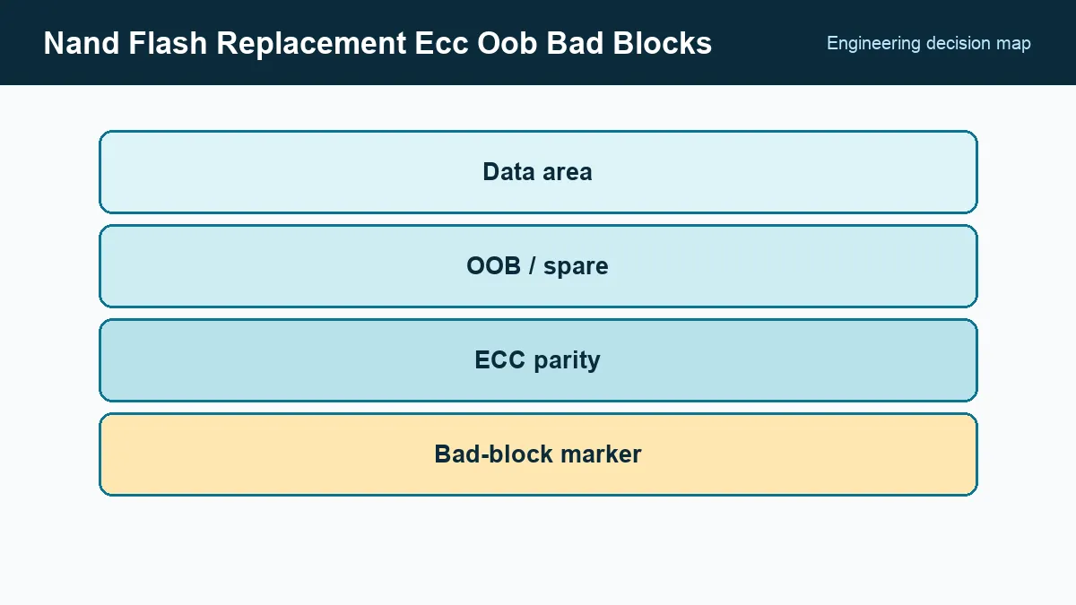
Reserve OOB bytes for error-correction code (ECC) parity, bad-block markers, and required metadata, then verify that the chosen controller layout fits the candidate’s spare area. Record the NAND’s required correction strength and codeword size; a bits-per-512-byte requirement cannot be compared with bits per 1,024 bytes without checking the supported code and layout.
The controller must support the polynomial or algorithm, codeword size, strength, and byte placement expected by every reader of the page. Boot ROM may use one fixed layout while the operating system uses another. If the first-stage loader cannot read the candidate reliably, a Linux driver update does not solve the boot failure.
NXP AN10860, accessed September 24, 2026, discusses NAND bad blocks and ECC considerations in embedded systems. Use the candidate data sheet for the exact ECC minimum and marker location; family-level guidance cannot replace those values.
Which programming tools must agree on NAND bad-block handling?
The offline programmer, bootloader, manufacturing utility, kernel driver, updater, and recovery tool must agree on the NAND’s bad-block markers and page/OOB layout. The candidate’s data sheet defines the marker locations and pages to inspect; factory programming must preserve those markers while writing ECC and application metadata.
Audit every tool that touches the image: offline programmer, bootloader, manufacturing utility, kernel driver, updater, and recovery tool. Verify that they agree on page/OOB layout, erase-block size, bad-block table format, and endianness. A raw binary image that includes spare bytes is often geometry-specific.

Start testing with devices that include factory-marked bad blocks. A perfect sample can let a broken skip algorithm pass unnoticed.
Exercise aging features and read recovery
Compare program/erase endurance, retention assumptions, read-disturb limits, partial-page programming restrictions, multi-plane rules, and maximum bad-block allowance. Check whether the device requires read retry, enhanced-status commands, or refresh policies as errors accumulate.
Use raw bit-error statistics before correction, corrected-bit counts, and uncorrectable events to assess margin. Run cycling and retention tests appropriate to the product rather than relying on an initial full readback. Power-interrupt program and erase operations to verify recovery and block retirement.
If on-die ECC is available, determine whether it can be disabled, how status is reported, and whether its hidden code conflicts with host ECC or OOB use. “ECC enabled” does not show that the boot ROM and flash filesystem share the same data contract.
How do you measure NAND read margin after wear?
Measure corrected-bit counts, raw bit-error data where available, and uncorrectable events relative to the controller’s ECC limit after representative cycling and retention stress. Compare the distributions with fresh devices and include patterns that expose disturb or coupling. A matching final readback alone hides how close the device is to exhausting correction capacity.
Define a refresh or retirement threshold below the uncorrectable point and verify that software can act on the reported error counts. If the candidate reports health differently, that interface is part of the substitution work.
Release the full software-hardware combination
The approved record should include NAND ordering code, geometry, ID table, timing mode, ECC requirement and layout, OOB map, bad-block-marker rule, controller configuration, boot-ROM constraint, driver versions, image format, programmer recipe, and reserved-block policy.
Qualification should cover blank-device programming, boot, updates, recovery, marked bad blocks, temperature and voltage corners, cycling, retention, read disturb, and interrupted operations. Procurement can then control the silicon together with the software baseline that makes it usable, instead of substituting by density and package alone.
Frequently Asked Questions (FAQ)
Can a stronger software ECC setting make any raw NAND compatible?
No. The controller must support the required correction strength, codeword, spare-area budget, and data layout. Boot ROM and existing images may impose a fixed ECC format that software cannot change.
Why must factory bad-block markers be preserved?
Raw NAND is shipped with permitted bad blocks identified in specified spare-area locations. Erasing or overwriting those markers can cause the flash-management layer to use unreliable blocks.
Does equal NAND capacity imply equal page and block geometry?
No. Page size, spare size, pages per block, planes, dies, addressing cycles, and ECC requirements can differ at the same nominal capacity.