Table of Contents
- Resolution sets the settling target
- How do source impedance and the RC filter limit SAR acquisition?
- Why is amplifier gain bandwidth insufficient to qualify a SAR ADC driver?
- How does a previous channel affect a multiplexed SAR ADC reading?
- Recheck protection and differential symmetry
- Prove the error at the sampling instant
A SAR ADC input is a switched-capacitor load, not a static high-impedance voltmeter. At the start of acquisition, the internal capacitor array connects to the input and draws a short charge pulse. The driver, source resistance, external filter, and previous channel state determine whether the input settles before conversion begins.
The visible symptom may be gain error, code-dependent distortion, or channel-to-channel memory. A DC multimeter at the ADC pin will not reveal it.
Resolution sets the settling target
For an ideal full-scale step, settling to half an LSB requires an error smaller than approximately 1/2^(N+1) of full scale for an N-bit converter. A 16-bit ADC therefore needs much tighter relative settling than a 10-bit ADC.
Allocate only part of that error to the input driver because reference error, ADC noise, distortion, and layout remain. Identify the actual maximum step: it may be full scale after a multiplexer change, or much smaller for a single continuous sensor channel.
Texas Instruments SBAA256, accessed September 24, 2026, provides a method for analyzing charge kickback and RC settling in precision SAR ADC inputs. Use the selected ADC’s acquisition capacitance and timing because they vary with sample rate, operating mode, and device family.
How do source impedance and the RC filter limit SAR acquisition?
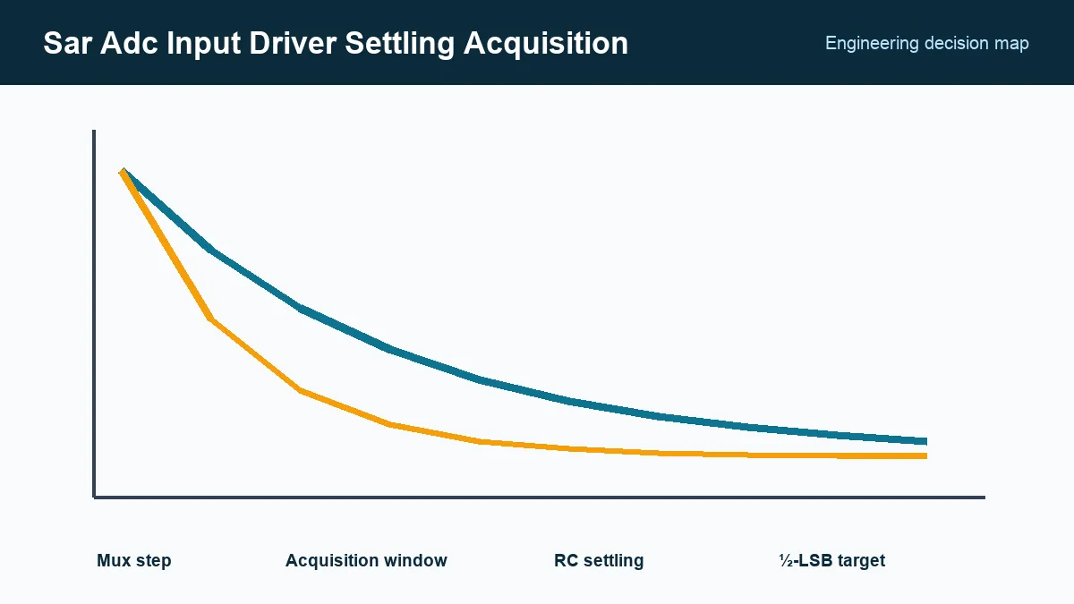
The full source impedance and RC network set how quickly the SAR input sampling capacitor can recover from charge kickback within the acquisition window. Include sensor resistance, protection resistors, multiplexer on-resistance, filter elements, amplifier output impedance, and PCB parasitics rather than evaluating the ADC-pin resistor alone.
A capacitor at the ADC pin serves as a local charge reservoir, while a series resistor isolates the amplifier from the switched load. Increasing either value changes bandwidth and settling. Too little capacitance allows a large voltage kick; too much can demand more charge than the amplifier supplies within the interval.
Analog Devices’ SAR ADC overview, accessed September 24, 2026, describes the sample-and-hold and successive-approximation cycle. Confirm when the external pin is acquiring versus converting; an advertised samples-per-second value does not reveal the whole acquisition window.
Why is amplifier gain bandwidth insufficient to qualify a SAR ADC driver?
Gain bandwidth does not by itself specify the amplifier’s settling to the ADC error target after a sampling-current pulse. Check large- and small-signal settling, output current, capacitive-load stability, output impedance, common-mode range, swing, noise, distortion, and saturation recovery at the intended sample rate and RC load.
The amplifier may see a repetitive pulse current at the sample rate. Its output impedance can rise with frequency, so a low DC output resistance is insufficient. The isolation resistor must be large enough for stability yet small enough to meet the acquisition error.
If the ADC has a differential input, maintain symmetry in impedance and capacitance. Common-mode movement and mismatch can convert into differential error even when each pin appears settled by itself.
How does a previous channel affect a multiplexed SAR ADC reading?
Charge left by the previous conversion can bias the next SAR sample before its input settles. A large switch from one rail toward a high-impedance channel near the opposite rail is a useful worst-case test because both the ADC and upstream multiplexer can retain charge.
Test the largest alternating channel step at the fastest scan rate. Options include extending acquisition, discarding the first conversion after a switch, buffering each channel, lowering filter impedance, or changing scan order. Firmware timing is part of the analog design when it controls acquisition duration.
Recheck protection and differential symmetry
Protection components also add leakage and capacitance. Verify them across temperature and signal range; a low-capacitance diode with high leakage can dominate a high-impedance sensor, while a low-leakage device can add too much sampling capacitance.
On a differential ADC, match protection, series resistance, and shunt capacitance on both pins. Unequal recovery after an overvoltage event or channel switch can create a differential error even when both inputs remain inside their absolute-maximum ratings.
Prove the error at the sampling instant
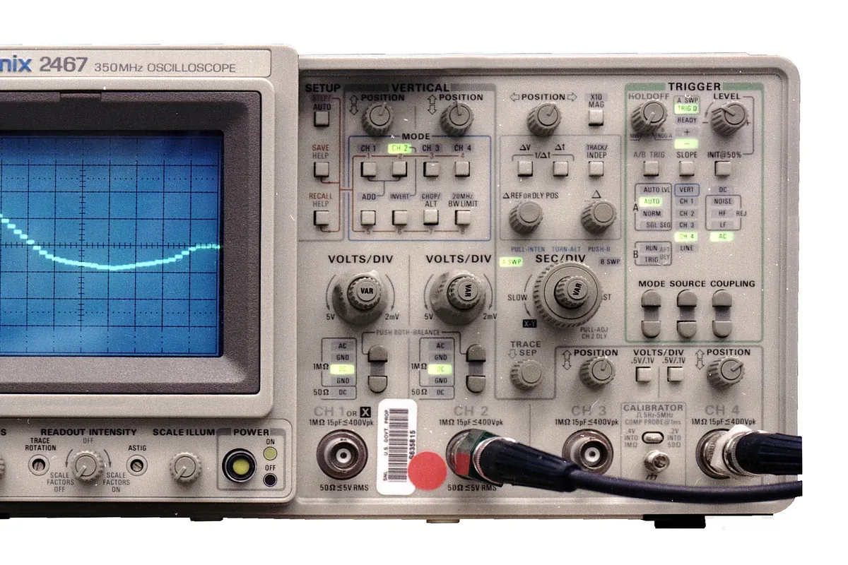
Direct probing can alter the RC network, so combine calculation, simulation, and measurement. Use a low-capacitance active probe where necessary and compare codes under controlled input steps. A coherent sine test can reveal dynamic distortion that a slow ramp misses.
Record ADC mode and sample rate, acquisition time, source range, maximum channel step, driver part, RC values and tolerances, multiplexer state, reference circuit, error allocation, and temperature range. Acceptance should cover DC code error, settling after a channel change, noise, and distortion. The resulting front-end specification remains valid when an amplifier, multiplexer, or filter component is proposed as an alternate.
Frequently Asked Questions (FAQ)
Why does a SAR ADC disturb its input at the start of acquisition?
Its internal sampling capacitor reconnects to the pin with charge left from the previous conversion. The external source and RC network must absorb that kickback and settle the sampling node before acquisition ends.
Can a large capacitor directly at the ADC input fix settling?
It can reduce instantaneous kickback, but it also increases the charge the amplifier must move, can reduce bandwidth, and may destabilize the amplifier. The capacitor and isolation resistor must be designed as a network.
How much settling accuracy is needed for an N-bit ADC?
A common initial target is less than one-half LSB at the sampling instant, then tighter limits may be assigned to the driver after reference, noise, distortion, and other errors consume part of the budget.