Table of Contents
- What Counts as the Multi-Chip Module Market — and Why Scope Changes the Numbers
- Multi-Chip Module Market Size and Growth Through 2035
- Demand Drivers: AI Accelerators, 5G, Automotive, and Miniaturization
- The Advanced-Packaging Bottleneck: CoWoS Capacity and Its Ripple Effect on MCM Supply
- Key Players: IDMs, Foundries, and OSATs Across the MCM Supply Chain
- Technology Routes: SiP, PoP, 2.5D Interposers, and Chiplet-Based MCMs
- What the Capacity Crunch Means for MCM Pricing, Lead Times, and Procurement
- Signals to Monitor: CoWoS Wafer Counts, Substrate Lead Times, and TSMC Capex
The multi-chip module market is a moving target before a single supplier or lead time enters the picture, because “multi-chip module” is not one defined category. Count only narrow multi-chip packages and the market reads $2.66 billion in 2025. Fold in system-in-package, chip-on-board, and package-on-package assemblies and the same market lands above $20 billion. Step back one level to the parent advanced-packaging market and the 2025 figure is $51.62 billion. Every one of these numbers is defensible; they answer different questions.
That scope gap is the first thing to resolve before any of these figures can inform a sourcing or investment decision, and it is the organizing idea of this piece. A buyer quoting the wrong scope can end up benchmarking against the wrong supplier set, the wrong package technology, and the wrong capacity constraint. The practical consequence is not academic: the tightest part of this market in 2026 sits in advanced packaging, where interposer and fan-out capacity determines which multi-chip modules are available at all.
This article is written for OEM, EMS, engineering, and procurement readers who need to size the multi-chip module opportunity and read its supply signals. It covers what counts as the MCM market, the size and growth forecasts through 2035, the demand drivers, the advanced-packaging bottleneck and its effect on MCM supply, the key players across the supply chain, the main technology routes, and what the capacity crunch means for lead times, pricing, and the signals worth monitoring.
What Counts as the Multi-Chip Module Market — and Why Scope Changes the Numbers

A multi-chip module packages two or more semiconductor dies inside a single component so they behave as one device on the board. That definition is broad enough to hold several distinct package families, and the label is applied inconsistently across marketing, datasheets, and market research. An industry packaging primer from AnySilicon treats the MCM as a family of approaches — side-by-side die placement, stacked die, and interposer-based assemblies — which is exactly why headline market sizes diverge.
The narrowest useful scope is the multi-chip package, or MCP, in which two or more bare dies are combined in one package without the full system-level integration of a system-in-package. Under that definition, TechSci Research sizes the market at $2.66 billion in 2025, rising to $5.46 billion by 2031. A broader definition that adds SiP, chip-on-board, and PoP assemblies — still legitimately “multi-chip modules” in common usage — pushes the same market above $20 billion for 2024 in MRFR’s accounting. Neither is wrong; the difference is scope, base year, and which package families are inside the count.
For sourcing purposes, the definitional detail matters more than the total. A 2.5D interposer module built on CoWoS-class capacity, a fan-out wafer-level package from an OSAT, and a commodity organic-substrate SiP share almost nothing in their supply chain, lead times, or supplier landscape. A market number that averages all three together will mislead anyone trying to plan around the constrained ones.
Multi-Chip Module Market Size and Growth Through 2035
Placed in context, the multi-chip module is a subset of the larger advanced-packaging market, which Mordor Intelligence estimates at $51.62 billion in 2025, growing to $90.11 billion by 2031. The MCM share of that total depends on how many of those advanced packages qualify as multi-die, multi-chip structures — the higher the die count and the more advanced the interposer, the more of that $51.62 billion is MCM-adjacent.
The narrow multi-chip-package segment’s own trajectory is the cleaner read for readers who want a like-for-like number. From a $2.66 billion base in 2025, TechSci’s forecast points to $5.46 billion by 2031, which implies a compound growth rate in the low-to-mid teens over that window. That is respectable but modest compared with the advanced-packaging parent, which is forecast to nearly double over a comparable period, because the parent includes the higher-value interposer and 2.5D/3D work driving AI compute.
Treat every one of these as a forecast with a base year and a stated window, not as a fact about today. The $2.66 billion is a 2025 estimate; the $5.46 billion is a 2031 projection; the $90.11 billion is a 2031 projection of a larger category. When the periods and scopes are aligned, the consistent story is that multi-chip integration is growing faster than the overall packaging market, with the growth concentrated in the advanced, interposer-based end rather than in mature organic-substrate modules.
Demand Drivers: AI Accelerators, 5G, Automotive, and Miniaturization

The strongest pull on the MCM market in 2026 is AI compute. Large accelerators are built from multiple dies — logic, I/O, and stacked high-bandwidth memory — assembled on a silicon interposer, because the reticle size of a lithography tool caps how large a single monolithic die can be. That structural limit makes multi-die packaging a requirement for leading-edge AI parts rather than a design choice, and it concentrates demand on exactly the interposer capacity that is scarcest.
Adjacent to AI, three other demand streams keep the broader MCM market moving. 5G radio and infrastructure systems use SiP and stacked assemblies to combine RF, power, and passive elements in a smaller footprint. Automotive modules pair logic with power and sensing in qualified, reliability-grade packages, which is why the qualification bar for these parts is higher than for consumer equivalents. And miniaturization in wearables, phones, and IoT edge devices favors chip-on-board and package-on-package structures that reclaim board area. These drivers pull on different package routes — organic-substrate SiP for cost-sensitive consumer designs, interposer and fan-out for compute — which is precisely why the aggregate market number is a poor guide to any single purchase.
Multi-die integration is not only a workaround for the reticle limit; it also changes cost economics. Heterogeneous integration lets a designer place the compute die on an expensive leading node while keeping I/O, memory controllers, and analog blocks on cheaper mature nodes, so aggregate silicon cost can come in below a hypothetical monolithic equivalent. The trade-off is test: every die must be screened as known-good-die before assembly, because a single defective die scrapped after packaging wastes the interposer, the substrate, and the assembly steps already performed. That known-good-die requirement is one reason advanced packaging carries a cost premium that raw market-size numbers do not reveal.
The Advanced-Packaging Bottleneck: CoWoS Capacity and Its Ripple Effect on MCM Supply

The most consequential supply constraint in the multi-chip module market is not the silicon itself but the advanced packaging behind it. TSMC’s CoWoS — chip-on-wafer-on-substrate — is the interposer route used for the highest-volume AI accelerators, and its capacity has trailed demand since the AI buildout accelerated. Secondary packaging-industry analysis tracking TSMC’s disclosures puts monthly CoWoS capacity at roughly 13,000 wafers at the end of 2023, expanding into a 30,000-to-35,000 range by mid-2024, with plans to approach 70,000 — figures best read as directional rather than precise, because TSMC updates them through capacity disclosures and investor briefings.
The ripple effect is allocation. TrendForce reported that NVIDIA locked in roughly 70% of 2025 CoWoS-L capacity, which tells the rest of the market where the scarce resource is going. Fan-out wafer-level packaging, the other workhorse for compact multi-die modules, tightened in parallel: MRFR’s electronic-packaging tracking describes OSAT fan-out slot lead times stretching past 50 weeks in 2024 with ASE and Amkor running near full. For a buyer, the takeaway is that interposer and fan-out capacity sets an effective ceiling on how many multi-chip modules the market can deliver, independent of wafer supply at the foundry.
Key Players: IDMs, Foundries, and OSATs Across the MCM Supply Chain
The multi-chip module market spans three different kinds of suppliers, and they do not compete on the same terms. Foundries, led by TSMC, control the highest-value interposer routes — CoWoS, InFO, and SoIC — and therefore gate supply for AI-class modules. OSATs such as ASE and Amkor operate the fan-out, SiP, and package-on-package lines that serve the broader commercial and automotive market, and their slot lead times are the leading indicator for the non-compute segment. IDMs and fabless product companies integrate dies into modules they design and sell as finished parts, which is where most buyers actually transact.
Among product-level suppliers, the picture is heterogeneous. Broadcom is central in networking and custom AI ASICs that ship as multi-die modules, while Analog Devices builds the RF, signal-chain, and power SiP modules that populate industrial, automotive, and communications designs. Other IDMs and fabless companies contribute SiP and stacked assemblies across power, sensing, and connectivity. The distinction that matters for sourcing is control: a foundry-led module, an OSAT-assembled module, and an IDM-designed module carry different traceability, different allocation behavior, and different second-source options. Our separate multi-chip module versus discrete procurement comparison covers that decision in detail.
Technology Routes: SiP, PoP, 2.5D Interposers, and Chiplet-Based MCMs
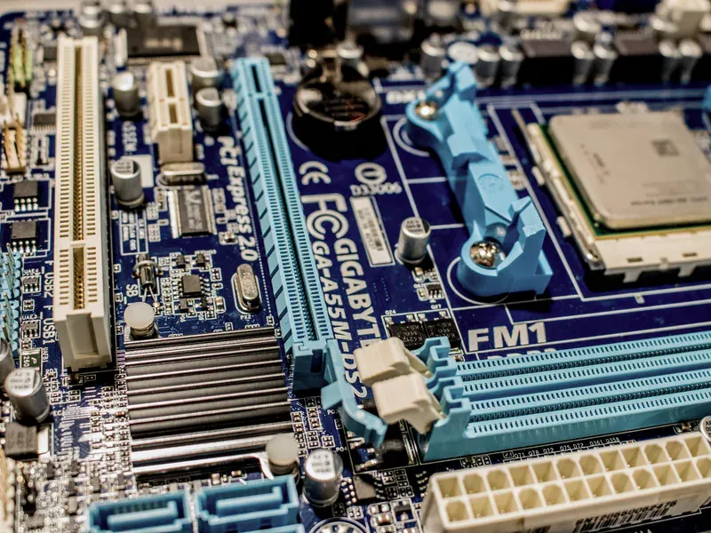
The term “multi-chip module” hides several distinct assembly technologies with different cost, performance, and supply profiles. Organic-substrate SiP places dies side by side or stacked on a conventional substrate, trading some interconnect performance for cost and broad OSAT availability. Package-on-package stacks one finished package on another — the classic case is memory over logic in mobile and embedded designs. 2.5D interposer assembly places dies on a silicon interposer with through-silicon vias, delivering the dense die-to-die bandwidth that AI accelerators require at the cost of scarce, expensive capacity.
Chiplet-based MCMs are the emerging intersection of these routes. Rather than integrating discrete dies, a chiplet architecture breaks a monolithic design into standardized blocks — compute, I/O, memory PHY — that are reassembled in a package. This is what makes 2.5D interposers so strategic: they are the physical layer that makes chiplet reuse practical at scale. For procurement, the technology route determines whether a module is a commodity with multiple assembly sources or a constrained part with a single dominant interposer path, and that single distinction outweighs most other factors in a supply plan.
For a buyer, the route decision usually reduces to three questions: what die-to-die bandwidth the design needs, what volume and cost target it must hit, and what reliability bar the end market imposes. High-bandwidth compute points to 2.5D interposers; cost-sensitive, space-constrained consumer designs point to organic SiP or package-on-package; and chiplet reuse pays off most where one base die can serve several products. The same system requirement can be met by more than one route, which is why the supply profile of the chosen route — not the module’s datasheet alone — belongs in the sourcing decision.
What the Capacity Crunch Means for MCM Pricing, Lead Times, and Procurement
The advanced-packaging bottleneck translates directly into procurement behavior in three ways. First, lead times for interposer and fan-out modules remain the market’s longest and least predictable, with the 2024 fan-out stretch past 50 weeks as the reference point for how far these can move when slots are full. Second, pricing on the constrained routes reflects allocation rather than component cost — buyers are paying for a position in the packaging queue as much as for the dies themselves. Third, second-sourcing is structurally limited, because the interposer and fan-out lines are concentrated among a small number of providers.
The practical response is to stop treating a multi-chip module as an interchangeable component and start treating it as a capacity-constrained part with a long qualification tail. Lock qualified second options before they are needed, because qualifying an alternative module can take 12 to 18 months once the dies or interposer change. Hold a dated, factory-acknowledged delivery date for the specific package route rather than a class-level lead time. And price the module against the total cost of the alternative — a discrete implementation or a redesign — not against last quarter’s unit price, since the capacity premium moves independently of silicon cost.
Signals to Monitor: CoWoS Wafer Counts, Substrate Lead Times, and TSMC Capex
Because the multi-chip module market is gated by packaging capacity, the most useful forward indicators are packaging signals rather than unit prices. Track TSMC’s disclosed CoWoS monthly wafer capacity — the 13,000-to-70,000 trajectory is the single clearest gauge of how much AI-class interposer supply is coming online. Watch OSAT fan-out and SiP slot lead times, with the 50-plus-week 2024 stretch as the alarm threshold to recognize. Monitor TSMC’s capital-expenditure guidance on advanced packaging, since new interposer capacity is the only durable fix for the bottleneck, and TrendForce’s press center publishes the capacity and allocation updates that track both.
The signals matter because they lead the visible market. Allocation announcements such as NVIDIA’s reported 70% of CoWoS-L capacity appear before downstream lead times lengthen and before module pricing reprices. A procurement team that watches wafer counts and slot lead times sees a tightening multi-chip module market months before it shows up as a delayed order or a repriced quote, and that is the difference between planning around the constraint and reacting to it.
Frequently Asked Questions (FAQ)
What is a realistic lead time for a multi-chip module order in 2026, and which package types are most supply-constrained?
Lead times vary sharply by package route rather than by a single market-wide figure. 2.5D interposer modules tied to CoWoS-class capacity, and fan-out wafer-level packaging slots, have been the tightest since at least 2024, when OSAT fan-out slots stretched past 50 weeks. Simpler organic-substrate SiP and PoP modules typically book shorter. Always request a dated, factory-acknowledged date for the specific package type rather than a class-level estimate.
Why do multi-chip module market size estimates differ by a factor of ten?
The estimates measure different scopes. A narrow multi-chip-package definition is $2.66 billion in 2025, while broad definitions that fold in system-in-package and chip-on-board assemblies exceed $20 billion, and the parent advanced-packaging market is $51.62 billion. Before using any figure, confirm which package types the report includes, its base year, and whether the number is historical, a forecast, or a compound growth rate.
How do I verify whether a multi-chip module was sourced through authorized distribution versus an independent channel?
Check the integrator's or manufacturer's current authorized-channel list for the region, and confirm that the quoting legal entity, location, product family, and the module itself fall within that relationship. For modules tied to foundry allocation, also ask whether the finished module ships through the manufacturer-recognized path or was reassembled or re-sourced through a third party, since both are common in the constrained package market.
How should I qualify a second source for a multi-chip module given foundry and OSAT capacity concentration?
Treat the module as a single integrated product whose constituent dies and interposer are not independently interchangeable. Qualify either an identical module from an alternative OSAT route, or a functionally equivalent module with different constituent dies, which typically requires a full 12-to-18-month qualification cycle. Because 2.5D and fan-out capacity is concentrated, keep a documented fallback option rather than assuming a second source will be available on demand.
What documentation should I request when sourcing multi-chip modules for automotive or medical applications?
Request lot-level traceability covering every constituent die and the interposer or substrate, not just the finished module label, plus the applicable qualification records such as AEC-Q100 for automotive parts, PPAP and change-notification commitments, and any medical-grade documentation the application requires. Confirm storage, moisture-sensitivity, and handling history, because a multi-chip module combines the pedigree requirements of several devices in one package.