Table of Contents
- Why can a lower-RDS(on) MOSFET make a replacement run hotter?
- Which gate-charge conditions belong in a replacement comparison?
- How do diode recovery and output capacitance affect compatibility?
- Separate mandatory limits from optimization preferences
- What evidence should close a MOSFET alternate approval?
A MOSFET cross-reference table can find parts with the same channel type, voltage rating and package. It cannot show whether the existing driver will switch the replacement cleanly or whether the board will remove its heat.
For a switching power stage, sourcing approval should compare conduction, gate-drive and commutation behavior together. A lower on-resistance can be attractive, but its benefit may be offset by larger gate charge, different capacitance or different body-diode recovery.
Why can a lower-RDS(on) MOSFET make a replacement run hotter?
The lower resistance reduces one conduction-loss term, but a replacement can increase switching-related loss or change the thermal path. The result depends on current, switching frequency, gate drive, dead time, parasitics and the installed package.
For a hypothetical conduction interval with 10 A current and 50% duty, changing on-resistance from 10 mΩ to 6 mΩ reduces the simple I²R × duty estimate from 0.50 W to 0.30 W. Those values assume the resistance used is appropriate to the operating temperature and gate voltage.
Now suppose total gate charge changes from 20 nC to 45 nC. At a 10 V gate swing and 200 kHz, the approximate gate-drive energy demand, QG × VGS × f, increases from 0.040 W to 0.090 W per device. That energy is distributed through the gate-drive path; it should not all be assigned to MOSFET junction heating. More importantly, a limited driver may produce different transition times.
This example is a screening comparison, not a complete efficiency calculation. It shows why the original resistance saving cannot be assessed independently.
Which gate-charge conditions belong in a replacement comparison?
Compare total gate charge and gate-drain charge at relevant drain voltage, current and gate swing. Also check the driver’s available current, gate resistance and the time allowed for each transition.
Infineon’s MOSFET data-sheet explanation separates gate-charge components and defines switching parameters under stated conditions. Moving a number into a spreadsheet without those conditions can create a false equivalence.
For initial review, use QGD divided by approximate available gate current to understand the scale of the Miller interval. Treat it as an estimate: driver impedance, plateau voltage and the circuit waveform affect the real transition.
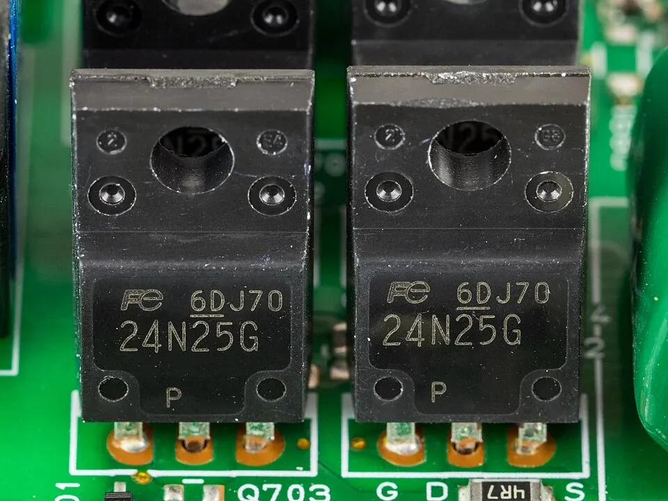
How do diode recovery and output capacitance affect compatibility?
In circuits that commutate a conducting body diode, reverse recovery can affect switching current, loss and overshoot. Output capacitance also exchanges energy during switching, and its voltage dependence makes a single capacitance number an incomplete model.
A candidate’s recovery charge should therefore be compared at relevant current, temperature and current slew rate. Check whether a stated switching-energy measurement includes recovery from another device. Adding separately calculated terms to an already inclusive measurement can double count loss.
The circuit’s dead time is another input. Too little dead time can permit cross-conduction; too much can extend diode conduction in some topologies. A replacement that changes transition behavior may need a timing review even if it is mechanically interchangeable.
Separate mandatory limits from optimization preferences
Before ranking price or loss, reject candidates that cannot satisfy the design’s required voltage margin, gate limits, temperature range, pinout and operating mode.
| Review layer | Approval input | Typical purchasing mistake |
|---|---|---|
| Static behavior | On-resistance at useful gate voltage and temperature | Comparing only 25°C typical values |
| Dynamic behavior | Gate charge, recovery and switching conditions | Treating lower resistance as a universal upgrade |
| Package and board | Thermal path, pad geometry and terminal functions | Relying on the package family name |
| Abnormal operation | Startup, short-circuit and required avalanche behavior | Assuming a headline current rating covers faults |
Linear operation needs a separate safe-operating-area review. A MOSFET suitable for efficient switching is not automatically suitable for prolonged linear stress.
What evidence should close a MOSFET alternate approval?
Close the approval with waveforms and temperature evidence from the relevant board configuration, along with the exact ordering-code comparison. Include startup, steady load, load transitions and the fault cases the design must tolerate.
Record gate-source and drain-source overshoot, switching behavior, efficiency or loss observations, and the temperature measurement method. Keep the driver settings and any changed resistors with the approval. If the alternate requires surrounding changes, procurement should release that configuration explicitly rather than labeling the device an unconditional drop-in replacement.
Frequently Asked Questions (FAQ)
Is gate-threshold voltage the correct value for choosing the gate drive?
No. Threshold is defined at a small specified current. Use the gate voltage associated with the required on-resistance and operating conditions, within the gate's permitted limits.
Can a package-name match establish pin compatibility?
No. Check the drawing, terminal assignment, exposed pad, source-sense connection and land pattern. Similar package labels can hide different connections.
Should an automotive qualification suffix be removed to improve availability?
Treat a grade or qualification change as a deviation requiring the program's approval. A similar base part number does not preserve every qualification, temperature or documentation requirement.