Table of Contents
A voiding percentage is a ratio, and a ratio without a denominator is not an acceptance criterion. The same “18%” can describe a small central void, a ring around the joint edge or a cluster under the hottest part of the die.
For QFN thermal-pad voiding, agree the inspection region, classification method and engineering acceptance before the first production lot. That makes a failed result actionable instead of turning it into an argument about an isolated number.
What should a voiding percentage measure?
It should measure the classified void area within a defined joint region, using a repeatable image and segmentation method. Record the denominator, total void area, largest individual void and their locations.
For example, an intended 4 mm × 4 mm joint region has an area of 16 mm². If the agreed method classifies 3.2 mm² as void, the reported area fraction is 20%. That arithmetic is useful only if both supplier and customer use the same region. Measuring against the entire package outline would produce a different and misleading result.
Define how the method treats thermal vias, edge exclusions and overlapping structures. Keep the original image and annotated region with the inspection record. If two machines or operators classify the same board differently, resolve the method before comparing lot trends.
TI’s QFN/SON attachment guide discusses land patterns, thermal vias, solder volume and reflow. It presents process-development guidance, not a universal acceptance percentage for every QFN application.
Location matters as much as area
Void location, joint thickness, thermal-via arrangement and the heat source above the joint all affect the heat path. Total area alone loses that spatial information.
A cluster beneath the hottest portion of a die can be more significant than the same area dispersed elsewhere. Voids near a joint edge may raise a different mechanical concern. The effect depends on the device and assembly; it cannot be reduced to “lower is always sufficient.”
The heat path runs from the die through the die attach, the exposed pad and the solder joint into the thermal vias, copper and board. An X-ray of the solder joint does not show the die-attach layer or every via connection, so a joint image should not be used to infer the temperature of the die by itself.
As a planning illustration, an additional 4°C/W of effective thermal resistance at 3 W would increase temperature by 12°C. This calculation shows why a thermal penalty can matter, but it does not assign 4°C/W to any particular void percentage. That relationship needs assembly-specific evidence.
Compare assemblies under the actual power and cooling conditions. Use the device maker’s specified temperature-estimation method or a validated thermal model, and retain margin below the relevant junction-temperature limit. A cool package top by itself does not establish the junction temperature.
How should the purchase specification define acceptance?
Combine measurable image criteria with thermal and reliability requirements approved for the product. Identify the applicable workmanship document and revision where the contract requires one; use its actual terms rather than a generic summary.
| Specification item | Required detail |
|---|---|
| Joint being inspected | Package/board revision, exposed-pad geometry and via layout |
| Imaging method | View, magnification, calibration and segmentation settings |
| Reported measures | Total area fraction, largest void, position and excluded features |
| Sampling and traceability | Inspection coverage, lot identity and response to an outlier |
| Engineering acceptance | Product-specific limits and required thermal/reliability evidence |
| Nonconformance response | Containment, engineering disposition and requalification scope |
Electrical attachment matters too. Some exposed pads provide an essential ground connection as well as a thermal path. Confirm the device’s requirements rather than treating the pad as optional metal under the package.
TI’s exposed-pad thermal-layout guidance explains the role of the board and thermal path. A generic package thermal-resistance value does not describe every board stack-up, copper area or airflow condition.
Correct the process behind a failed lot
When a lot fails the agreed criteria, contain the affected material and compare paste, stencil, board finish, via treatment, placement and recorded reflow conditions with the approved process. Change a controlled variable and inspect the resulting assemblies before releasing the correction.
Excess paste can alter stand-off or encourage floating; insufficient paste can leave poor attachment. Via treatment and reflow behavior can also affect void formation. Use the exact package guidance and paste supplier’s process window, then validate the result on the actual assembly.
If old component stock is suspected, use a separate solderability review instead of attributing every void to component age. A good incoming solderability result also does not qualify an unsuitable stencil or reflow profile.
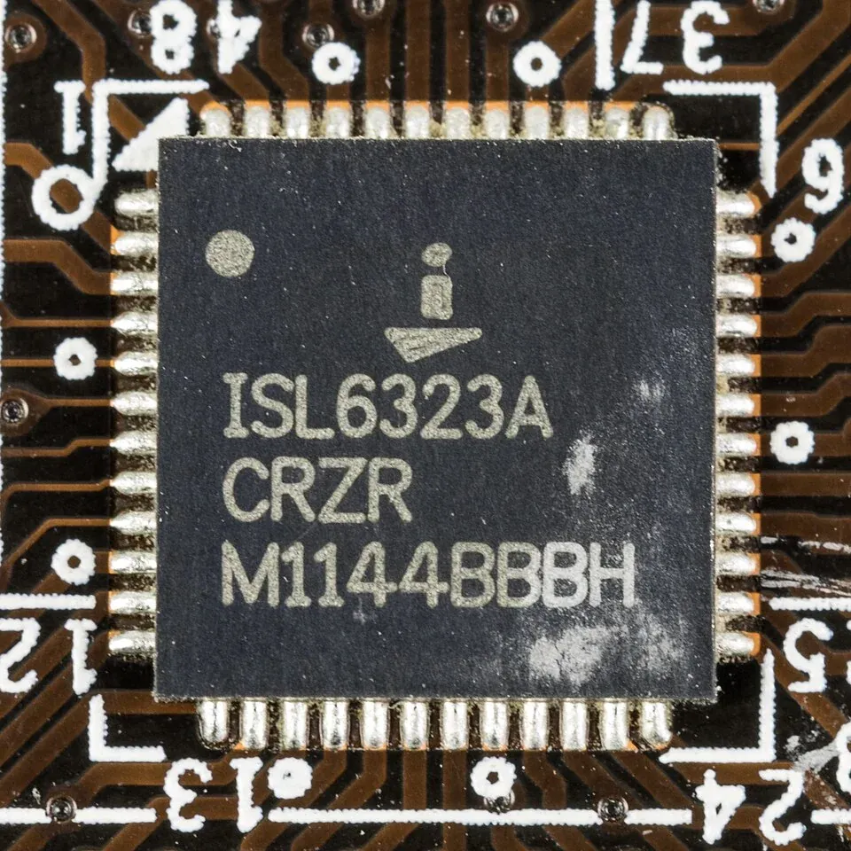
For component sourcing and quality review, keep the package suffix, finish, moisture classification and lot records available to the assembly team. Start from the TI brand page to confirm the exact suffix before comparing assembly data. The final release decision should be tied to the accepted joint requirements and test evidence; a concession that is not limited to the affected configuration and lot is not a controlled release.
Frequently Asked Questions (FAQ)
Is every bright region in an X-ray a solder void?
No. Image appearance depends on the imaging setup, materials, vias and overlapping structures. Define the inspection region and classification method using the assembly drawing and representative images.
Can visible side fillets prove that the exposed pad is adequately soldered?
No. The central joint is hidden under the package. Side-joint appearance and exposed-pad attachment are separate inspection questions.
Should a voiding result from a different package establish the acceptance limit?
No. Use the exact device guidance, board construction, power dissipation and reliability requirements. Results from another package can inform an investigation but do not establish equivalence.
Does IPC-A-610 define a universal void limit for QFN thermal pads?
No. The applicable workmanship standard and revision, together with the device guidance, board construction, power dissipation and reliability requirements, define what is acceptable for the product. A number copied from another package is not a substitute for that review.