Table of Contents
- Convert the Rail Requirements Into a Converter Envelope
- Choose an Integrated Converter, Controller, or Power Module
- Check Duty-Cycle Limits at Both Input Extremes
- Size the Current Path for Steady Load and Transients
- Trade Switching Frequency Against EMI and Thermal Loss
- Compare Guaranteed Conditions, Not Feature Labels
- Validate the Final Board Before Approving an Alternate
A buck converter shortlist should begin with operating corners, not with a current rating copied from a product table. The device must regulate the rail at both ends of the input range, carry the real transient current, remain inside its control-loop and external-component limits, and release heat through the final PCB.
That distinction matters when an alternate is being considered. Two parts can share the same nominal input voltage, output voltage, switching frequency, and advertised current yet behave differently during dropout, pulse skipping, current limit, startup, or a fast load step. The approval unit is the complete converter on its board, not the IC in isolation.
Convert the Rail Requirements Into a Converter Envelope
Write the input range at the IC pins, including source tolerance, cable and connector drop, upstream protection loss, startup overshoot, and any surge that the converter is expected to survive. Then define the output tolerance at the load, static current, repetitive peaks, load-step slew rate, startup load, allowed ripple, sequencing, ambient range, airflow, and available board area.
Keep survival and regulation conditions separate. Absolute-maximum voltage is not a continuous operating recommendation, and a converter that survives a transient may not hold its output in regulation during that event. Likewise, the headline output-current value is normally conditional on input/output voltage, switching frequency, inductor, package, layout, and temperature.
The TI buck-converter portfolio and the manufacturer’s buck step-down selector can narrow candidates, but the selected data sheet must answer the corner cases. ST and Analog Devices organize their buck families differently, so normalize every candidate into the same system-level envelope before comparing them.
Choose an Integrated Converter, Controller, or Power Module
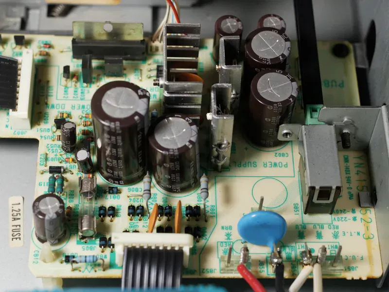
An integrated converter usually combines the control loop and power MOSFETs. It reduces power-loop area and component count, but switch resistance, current limit, and thermal concentration are fixed by the IC. A controller uses external MOSFETs and can scale to higher power or distribute heat, at the cost of gate-drive, layout, compensation, and MOSFET selection work. A power module may also integrate the inductor or other passives, trading a simpler layout for package height, sourcing concentration, and less freedom to change the power stage.
Choose among these architectures before comparing individual part numbers. A pin-compatible integrated converter is not an alternate for a controller that expects external FETs. Even within integrated devices, asynchronous and synchronous topologies differ: a synchronous device replaces the catch diode with a controlled low-side MOSFET, which can improve efficiency but adds dead-time and reverse-current behavior that must match the application.
The Analog Devices buck regulator and controller catalog keeps both architectures visible. Use that distinction in the approved-vendor list so procurement does not treat all entries under “buck regulator” as one interchangeable commodity.
Check Duty-Cycle Limits at Both Input Extremes
The ideal steady-state duty cycle is approximately output voltage divided by input voltage, but a real converter loses voltage across its switches, inductor, and interconnect. At low input voltage, maximum duty cycle and minimum off-time can force the converter into dropout. At high input voltage, the on-pulse required for a low output may be shorter than the IC’s minimum on-time.
For each candidate, calculate the required duty cycle at minimum input and maximum load, then at maximum input and minimum load. Compare it with guaranteed minimum on-time, minimum off-time, switching-frequency tolerance, dropout behavior, and any frequency-foldback mode. A 24 V-to-1 V rail is often limited by minimum on-time at high line; a 5 V-to-3.3 V rail may be limited by dropout at low line.
Do not assume that selecting a higher nominal switching frequency is harmless. The on-time becomes shorter as frequency rises, and switching loss usually increases. Some parts allow frequency programming or synchronization, while fixed-frequency order codes can look nearly identical. Exact suffix control belongs in the BOM review, not in a note added after a substitution arrives.
Size the Current Path for Steady Load and Transients
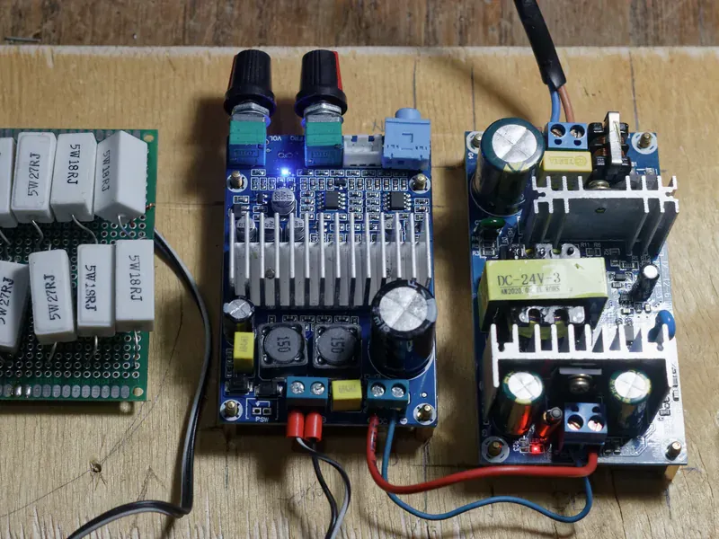
Average load current does not equal switch peak current. Inductor ripple adds to the load at the high point of every switching cycle, and a transient can demand more current before the feedback loop raises the duty cycle. Select inductance from ripple, transient response, physical size, saturation behavior, core loss, and the range permitted by the regulator’s data sheet.
Compare inductor saturation current with the converter’s worst-case peak current limit, not with nominal load alone. Also check RMS current, winding temperature, DCR loss, and whether soft saturation or abrupt saturation is assumed. Output capacitors must meet capacitance after DC-bias derating and temperature, along with ESR and ripple-current requirements. A ceramic capacitor marked 22 µF may provide materially less capacitance at its operating bias.
Current limit needs a system interpretation. Cycle-by-cycle limiting, hiccup, latch-off, and frequency foldback place different stress on the IC, inductor, input source, and downstream load. Coordinate the buck response with the upstream eFuse fault strategy so two protection loops do not create repeated brownout and restart cycles.
Trade Switching Frequency Against EMI and Thermal Loss
Higher frequency can reduce inductance and capacitance, but it increases the number of switching transitions per second. Lower frequency can reduce switching loss while requiring larger magnetics and potentially moving ripple into a less convenient band. The best setting depends on efficiency targets, transient requirements, acoustic limits, EMI filter size, synchronization needs, and the permitted component footprint.
Use the efficiency graph only when its input, output, frequency, inductor, and temperature conditions resemble the design. For a first thermal model, account for high-side and low-side conduction loss, switching loss, gate-drive and control loss, inductor copper/core loss, and capacitor ESR. Then measure the assembled board. Junction-to-ambient figures from a standardized test board do not reproduce every enclosure or copper layout.
If the voltage drop is small, current is modest, and noise or simplicity dominates, an LDO regulator may be appropriate. Where the LDO would dissipate excessive power, a buck stage can perform the large conversion and an LDO can provide final filtering. That is an architecture decision, not evidence that one regulator can replace the other.
Compare Guaranteed Conditions, Not Feature Labels
Create a normalized candidate table with input operating range, output range, guaranteed current-limit bounds, minimum on/off time, dropout behavior, switching-frequency tolerance, control mode, compensation method, output-discharge behavior, soft-start, power-good thresholds, quiescent current, shutdown current, package, temperature grade, and qualification status.
Control-loop implementation matters. Internally compensated parts restrict the acceptable inductor and output-capacitor region. Externally compensated controllers allow tuning but require a validated compensation network. Constant-on-time, peak-current-mode, valley-current-mode, and voltage-mode control can respond differently to input feed-forward, low-ESR capacitors, pulse skipping, and synchronization.
Record whether a value is minimum, typical, or maximum and the temperature at which it applies. The Richtek buck selection guidance illustrates why input/output conditions, frequency, efficiency, transient response, and layout need to be considered together. A feature checkbox such as “forced PWM” or “low IQ” is useful only after its operating conditions match the product’s modes.
Validate the Final Board Before Approving an Alternate
Test startup at low and high input, with no load, normal load, and the worst allowed pre-biased output. Apply load steps with the specified edge rate and observe output deviation, switch-node behavior, inductor current, and recovery. Repeat line steps, shutdown, restart, current limit, output short, and recovery while monitoring the upstream rail.
Measure ripple with a short ground connection and declared bandwidth. Run efficiency and thermal tests across relevant loads and enclosure conditions, not only on an open bench. Conducted and radiated emissions must use the production input filter, cabling, grounding, and switching-frequency configuration.
For an alternate, compare pin functions as well as pin numbers: enable thresholds, power-good structure, feedback reference, soft-start capacitor, mode selection, exposed-pad connection, and unconnected-pin instructions. Update the controlled schematic, layout review, orderable code, test record, and approved conditions together. That evidence makes a buck converter substitution repeatable instead of relying on a matching voltage-and-current label.
Frequently Asked Questions (FAQ)
What is the difference between a buck converter IC and a buck controller?
A buck converter IC commonly integrates the control circuit and power switches, while a buck controller drives external MOSFETs. Controllers give the designer more freedom over voltage, current, switching loss, and thermal placement, but they require a larger external power-stage design and qualification effort.
Why can a buck regulator fail to regulate at a valid input voltage?
The input can be inside the headline voltage range while the required duty cycle violates minimum on-time, minimum off-time, dropout, current-limit, or thermal conditions. Check those limits at input, load, switching-frequency, and temperature extremes rather than relying on the absolute input range.
Can two buck converter ICs with the same voltage and current ratings be substitutes?
Not without further verification. Minimum on-time, compensation, current-limit behavior, pin functions, light-load mode, startup, package thermal performance, external component limits, and fault recovery can differ enough to require a schematic, layout, firmware, or validation change.