Table of Contents
An I2C level shifter sits between two voltage domains, but it remains part of one wired-low protocol. Every device may pull a line low; pull-up networks return the lines high; arbitration and clock stretching depend on that behavior remaining visible through the translator. A part that moves a push-pull logic signal between 1.8 V and 3.3 V is not automatically suitable.
Start with the electrical behavior on both sides, then decide whether the system needs voltage translation, capacitance buffering, fault segmentation, or galvanic isolation. These are different jobs even when the catalog places the devices in adjacent interface categories.
Confirm Both Sides Behave as Open-Drain Buses
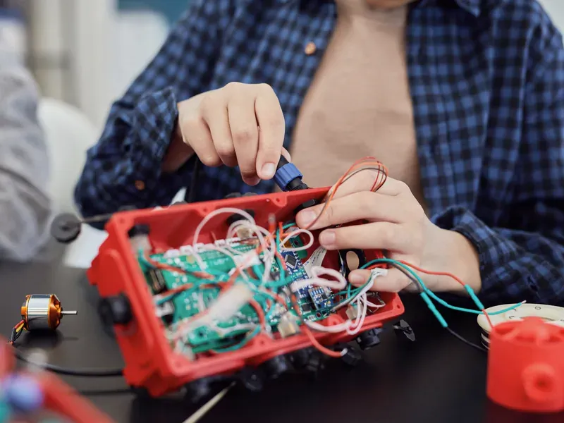
List every controller and target on SDA and SCL. Confirm their I/O modes, low-level sink capability, input thresholds, clock-stretch behavior, arbitration requirements, and maximum bus frequency. A target that drives SCL low during clock stretching must be able to propagate that state back to the controller.
Passive FET translators exploit the open-drain structure and can pass a low in either direction without a direction pin. Edge accelerators, buffers, and auto-direction logic translators use different detection methods and can impose minimum pulse, offset-voltage, or drive-strength conditions. The exact datasheet must state I2C or SMBus support for the intended mode.
The NXP AN11127 application note describes NVT20xx and PCA9306 bidirectional voltage translators and discusses device operation and resistor sizing. It is a useful architecture reference, but the permitted voltage relationship and bias circuit still come from the selected part and revision.
Check Voltage Domains and Power-Off States
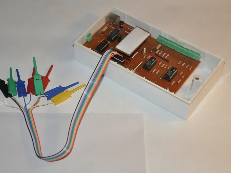
Use minimum and maximum rail values rather than nominal labels. Review input-low and input-high thresholds, pull-up voltage, clamp or reference pins, enable thresholds, and absolute maximum conditions for every combination of rail tolerance.
For example, the TI PCA9306 product page identifies it as a two-bit bidirectional I2C/SMBus voltage translator and lists 1.2 V to 3.3 V on VREF1 and 1.8 V to 5.5 V on VREF2, with VREF1 not exceeding VREF2. Those ranges describe PCA9306, not a generic wiring rule for all translators.
Power sequencing needs explicit states:
| State | Question to answer |
|---|---|
| Both domains powered | Are logic thresholds and low-level margins valid? |
| Low-voltage side off | Can a pull-up or signal back-power the unpowered rail or I/O? |
| High-voltage side off | Does the translator isolate, clamp, or leak through? |
| Translator disabled | Are both bus segments released to their pull-ups? |
| Brownout or slow ramp | Can a partially biased circuit hold SDA or SCL low? |
Do not rely on “Ioff,” “powered-off protection,” or “high impedance” without checking which pins and voltage conditions the statement covers. If a sensor board may be removed while the controller remains energized, include connector sequencing and hot-plug transients.
Calculate Pull-Ups on Each Side
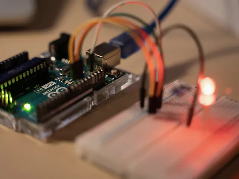
Each side normally needs a pull-up to its own logic rail. The resistor must be low enough to charge the total capacitance within the required rise time, yet high enough that every device can pull the line below the guaranteed input-low level without exceeding its sink-current limit.
The rise-time relationship for a first-order RC bus is commonly approximated using the product of pull-up resistance and bus capacitance. The exact coefficient depends on the voltage points used by the relevant I2C mode. Follow the applicable bus specification and the translator’s guidance rather than inventing one universal resistor value. TI’s I2C pull-up calculation note lays out the minimum and maximum constraints.
Build the capacitance budget from controller pins, target pins, translator channels, connectors, cable or flex, ESD devices, test fixtures, and PCB traces. Include component tolerance and effective capacitance under bias where relevant. Existing pull-ups on modules appear in parallel; two 4.7 kΩ resistors become approximately 2.35 kΩ, which can violate sink-current limits even if either resistor would work alone.
Measure the rising edge at the farthest or most heavily loaded nodes. A clean waveform beside the controller does not prove the remote target receives the same timing margin.
Decide Whether Translation, Buffering, or Isolation Is Needed
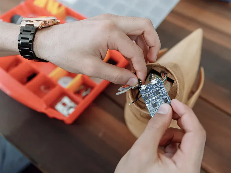
A translator solves incompatible logic-high voltages. A buffer or repeater can split capacitance, change low-level behavior, support hot insertion, or isolate a stuck segment, depending on its architecture. A switch or multiplexer can resolve address conflicts or disconnect branches. A digital isolator breaks the galvanic connection and needs isolated power and isolation evidence.
| System problem | Likely device class | Additional check |
|---|---|---|
| 1.2 V controller to 3.3 V targets | I2C level translator | Reference-voltage relation and pull-ups |
| Excess total capacitance | I2C buffer/repeater | Segment limits and offset compatibility |
| Duplicate target addresses | I2C switch/multiplexer | Channel control and startup state |
| Remote board with ground offset | I2C isolator | Working voltage, timing, and isolated power |
| Field-replaceable branch | Hot-swap buffer or switch | Precharge, stuck-bus, and connector sequencing |
If the actual requirement is to add remote digital inputs and outputs rather than translate the bus, use the GPIO-expander selection process and review its interrupt, reset, partial-power, and register-map behavior separately.
The digital-isolator selection guide covers working voltage and insulation evidence. Do not claim galvanic separation for a level shifter merely because the voltage domains are different.
Validate Protocol Corner Cases
Test at minimum and maximum rail voltage, temperature, clock frequency, and capacitance. Exercise writes, reads, repeated starts, clock stretching, multi-controller arbitration where used, and reset while either SDA or SCL is low. Power each domain in both orders and remove power while transactions are active.
Capture low-level voltage, rise time, fall time, propagation delay, and any pulse distortion on both sides. If a buffer uses different low-level offsets on its ports, verify that cascaded devices recognize one another. Also confirm that a stuck target cannot permanently prevent the controller from executing the intended recovery sequence.
For a BOM review, keep controller and target voltage limits, bus speed, calculated capacitance, pull-up population, translator ordering code, and power-sequence assumptions together. Candidates from the NXP or TI catalogs still require review of the exact package, enable behavior, frequency, and qualified operating range.
The approval boundary should state what can change without a new bus test. A package option, translator architecture, ESD component, connector, cable length, module, or pull-up value can alter the electrical network even when firmware and device addresses remain unchanged.
Frequently Asked Questions (FAQ)
Can any bidirectional logic level shifter be used for I2C?
No. I2C uses open-drain signaling, wired-low arbitration, and clock stretching. Choose a translator or repeater whose architecture and datasheet explicitly support those behaviors at the required voltage and speed.
Does an I2C level shifter need pull-up resistors on both sides?
Most passive and open-drain translation arrangements require each voltage domain to have its own pull-up path. Calculate each side from its logic thresholds, sink-current limit, total capacitance, and rise-time requirement.
When should an I2C buffer be used instead of a level shifter?
Use a buffer or repeater when the bus needs capacitance segmentation, stronger edge control, hot-swap behavior, or stuck-bus support. Voltage translation alone does not automatically isolate one segment's capacitance or faults.