Table of Contents
A stable meter reading can hide reference disturbance in the first conversions of a burst. The REF pin of a successive-approximation-register analog-to-digital converter (SAR ADC) can draw short charge pulses that a slow measurement averages away.
This is a reference-drive problem with a conversion-dependent load. It is separate from the analog-input driver and acquisition-time problem, even when both errors appear in the same output codes.
Charge redistribution moves the REF node during conversion
The SAR conversion process redistributes charge internally, drawing transient current from the reference path. Local charge storage, driver impedance and recovery time determine how much the reference moves while the converter makes its decisions.
Analog Devices’ precision SAR reference-design article explains the reservoir-capacitor and reference-buffer roles. The appropriate circuit depends on the converter: follow its required reference capacitance, drive conditions and layout guidance rather than applying one capacitor value to every SAR ADC.
Begin with the converter’s conversion cadence and operating modes. A steady stream, a long idle followed by a burst, and multiplexed channels can stress the reference differently. A test at one average sample rate can miss the most demanding short interval.
How can you estimate the initial droop and recovery requirement?
Use charge divided by effective capacitance for an initial droop estimate, then model recovery using the actual driver and network. This is a screening calculation; a switched-capacitor load and active buffer do not necessarily behave as a single linear RC.
For an illustrative pulse of 20 nC into 10 µF of effective local capacitance:
ΔV = Q / C = 20 nC / 10 µF = 2 mV.
Suppose an 18-bit converter uses a 4.096 V reference, and the allocated reference error at the relevant decision time is one-quarter of an ideal LSB. One LSB is 15.625 µV, giving an allocation of about 3.91 µV. The 2 mV disturbance is much larger than that allocation.
If recovery were a first-order exponential, reaching 3.91 µV from 2 mV would require t ≥ τ × ln(2000 / 3.91), or approximately 6.24 time constants. The actual circuit must be assessed against its load waveform, effective capacitance, damping and buffer stability. These assumed values are not an LTC6655 or ADC test result.
At lower input codes, a given reference error can have a different output-code consequence. Start with the demanding full-scale condition, then exercise the signal range and sequences the application actually uses.
Which changes improve the reference path without hiding another problem?
A local reservoir, a suitable buffer and a low-impedance layout can reduce conversion disturbance, but each change must preserve stability and startup behavior. Increasing capacitance blindly can trade a burst problem for excessive startup time or buffer instability.
| Candidate change | Expected benefit to investigate | Countercheck |
|---|---|---|
| More effective local capacitance | Smaller initial charge-induced droop | DC-bias derating, ESR, startup and stability |
| Reference buffer | Better transient current delivery | Output swing, capacitive-load stability and added noise |
| Shorter REF/return paths | Less parasitic impedance | Probe arrangement and ground-current routing |
| Different conversion schedule | More time for recovery | Throughput and first-valid-sample requirements |
An LTC6655 series choice should therefore be evaluated in the intended reference circuit. Its static precision specifications do not establish every possible ADC interface. The reference error-budget pillar remains the place to allocate DC, drift and noise contributions.
How do you identify the first valid sample in a burst?
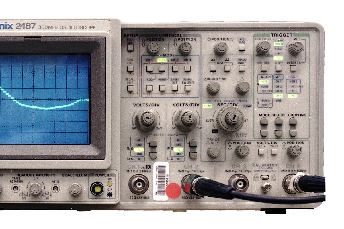
Capture the REF waveform and output-code behavior across the idle-to-burst transition, then determine when both meet the application’s error allocation. Compare the first sample, later samples and the steady-state stream under the same input condition.
Use a stable input near the demanding operating point, and vary burst length, idle interval and conversion rate deliberately. If discarding early samples is acceptable, define the rule from the demonstrated settling behavior and its operating corners. Do not assume that a fixed discard count is portable across capacitor substitutions or firmware timing changes.
The release record should preserve converter configuration, reference and buffer ordering codes, capacitor technology and effective value, layout revision, conversion timing and measurement setup. That record gives procurement a concrete reason to reopen validation when an apparently small reference-path component changes.
Frequently Asked Questions (FAQ)
Is reference settling the same as analog-input acquisition settling?
No. The analog input must settle while the input sampling network acquires the signal; the reference supports charge redistribution during conversion. Their loads and timing windows differ.
Can averaging remove reference droop?
Averaging can reduce uncorrelated random noise, but it does not reliably remove repeatable code-dependent or burst-dependent reference error. Correct the reference path or account for the demonstrated error.
Should a large probe capacitance be included in the test record?
Yes. Probe loading can change the reference node being measured. Use an appropriate measurement arrangement and record its loading, bandwidth and connection point.